
PRODUCT
PRODUCT
CONTACT US
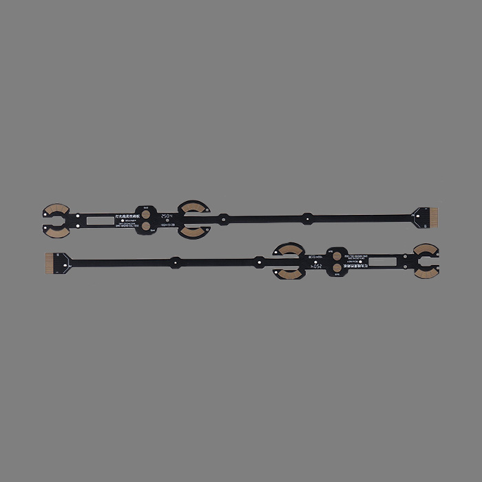


Commodity Name: Flexible Printed Circuit Board For Industrial Control Screen
Brand Name: HFast
Layers: 2L
Board Thickness: 0.20mm
Minimum Hole Size: 0.20mm
Minimum Line Width: 0.10mm
Minimum Line Spacing: 0.076mm
Range of Copper Thickness: 2-9oz
Density: 3.7g/cm3
Flexural Strength: 466-496Mpa
Surface Roughness: 0.3-0.5
Thermal Conductivity: >170
Dielectric Strength: >15KV/mm
Dielectric Constant: 9.0Mhz
Surface Treatment: Gold Plating
Color: Yellow Film and White Legend
Brief Introduction of Flexible PCB
Flexible Printed Circuit Board (FPC), also known as "soft board", is a type of printed circuit board made of flexible insulating substrates. It achieves three-dimensional spatial bending, folding, and dynamic adaptability that traditional rigid PCB cannot achieve through unique material and structural design, becoming one of the core technologies for miniaturization, lightweight, and high reliability of modern electronic products.
FPC has become a key technology for high-density electronic integration, especially in foldable devices, precision medical instruments, and next-generation automotive electronics, due to its spatial adaptability and dynamic reliability. Its design must strictly follow bending specifications and balance material selection between cost and performance. With the maturity of new processes such as mSAP precision etching and polymer thick film, flexible PCB will further evolve towards low cost, ultra-thin, and multifunctional integration, becoming the core carrier of intelligent hardware innovation.
Characteristics of FCB
1. Flexibility and bendability;
2. Lightweight and lightweight;
3. High density interconnection;
4. Excellent dynamic bending reliability;
5. Good heat dissipation performance;
6. High degree of design freedom;
7. Shock absorption and impact resistance performance;
8. Stable electrical performance.
Manufacturing Process of FCB Printed Circuit Board
The manufacturing of multi-layer PCB is much more complex than single/double-sided boards, and the main steps include:
1. Inner layer production: Perform pattern transfer (exposure, development), etching, and AOI testing on each inner core board.
2.Layering:Accurately align and stack the etched inner core board, semi cured sheet, and outer copper foil in the designed stacking sequence, and press them together into a whole under high temperature and high pressure.
3. Drilling: Drilling through holes, blind holes, and buried holes (the latter two usually require step-by-step drilling).
4. Hole metallization:By chemical copper deposition and electroplating processes, a conductive copper layer (PTH Plated Through Hole) is deposited on the hole wall.
5. Outer layer graphic transfer and electroplating: Perform graphic transfer on the outer layer, and then perform graphic electroplating (thickening the circuit and hole copper).
6. Etching:Etch off the copper foil that is not protected by the corrosion-resistant layer, forming the outer layer of the circuit.
7. Solder mask:Apply solder mask ink (green oil or other colors) to protect the circuit and prevent welding short circuits.
8. Surface treatment: Apply solderable/protective coatings (such as HASL, ENIG, OSP, tin deposition, silver deposition, etc.) on exposed solder pads.
9. Silk screen printing:Printing text symbols such as component part numbers and identification.
10. Electrical testing and final inspection: Conduct flying needle testing or needle bed testing to verify connectivity, and conduct final inspections such as appearance and dimensions.
Design key specifications of Flexible Printed Circuit Board
1. Bending design
-The dynamic bending area must use a single panel to avoid through holes; Bending radius ≥ 6-10 times the thickness of the plate.
2. Wiring optimization
-The corner of the wire adopts arc transition(non right angle) to reduce stress concentration; Arrange solder pads to avoid bending areas.
3. Pad strengthening
-QFP/BGA corner solder pads need to be reinforced with "tear drops"; Add reinforcement plates underneath the load-bearing components such as LEDs.
4. Impedance control
-High frequency circuits require calculation of dielectric thickness/line width, and low dielectric constant adhesive materials (such as polyethylene) should be selected.
Cost and Economic Analysis of Flexible Printed Circuit Board
-The main reason for high cost is that the price of PI substrate is 4 times that of FR4; Rolled copper is 30% more expensive than electrolytic copper; The yield of microporous process is low.
-Cost Reduction Trend:
-Polymer thick film method: PET substrate+conductive ink printing, with a cost only 1/10 of PI board, suitable for low-frequency scenarios such as control panels.
-Popularization of adhesive free technology: Laser direct copper-clad (LDI) is gradually replacing adhesive, improving yield and reducing thickness.
Development Trends of Flexible Printed Circuit Board
Development Trends
1. Ultra thin: The thickness is developing towards 0.05mm, suitable for micro devices (such as medical implants).
2. Mixed material: Balancing cost and performance between PI and PET composite substrates.
3.Integration: Integration with sensors/antennas (such as smart fabrics).
4. Green Manufacturing: Promote lead-free processes and comply with environmental regulations.
Online Message
Application


CONTACT US
Please use the form below to get in touch.
If you need a reply we will get in touch as soon as possible.