
PRODUCT
PRODUCT
CONTACT US
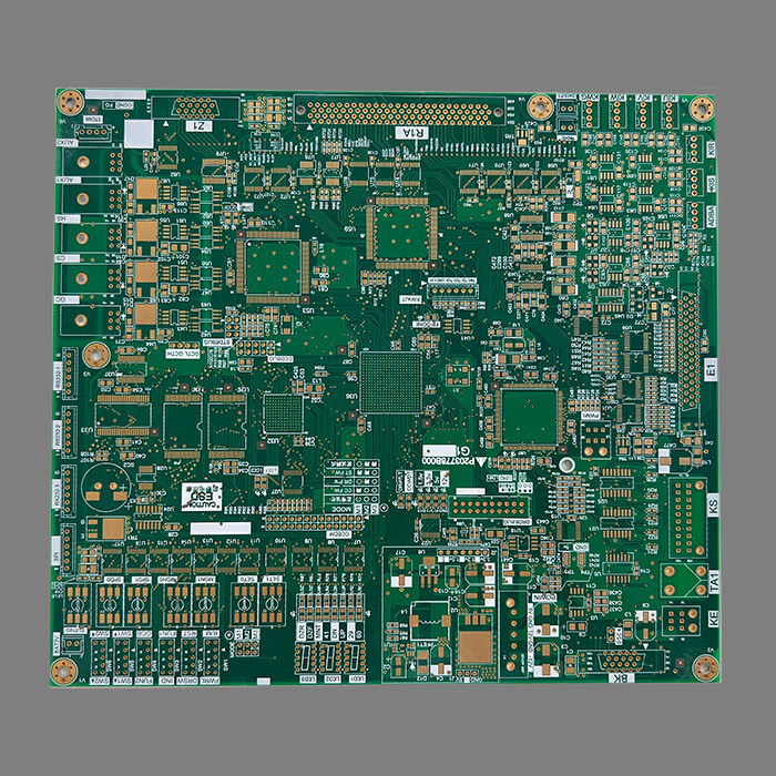


Key Parameters of Multilayer PCB
Commodity Name: Multi- layer Printed Circuit Board for Industrial Testing Equipment
Place of Origin: Jiangsu, China
Brand Name: HFast
Layers: 10L
Board Thickness: 2.0mm
Minimum Hole Size: 0.25mm
Minimum Line Width: 0.13mm
Minimum Line Spacing: 0.13mm
Surface Treatment: Gold Plating
Color: Green Oil and White Legend
Advantages: CEM1 Material, Fire Resistance Grade: 94V-0
Brief Introduction of Multi-layer PCB
A multi-layer PCB board is a printed circuit board (PCB) made by alternately laminating and bonding three or more layers of conductive copper foil pattern layers and insulation material layers together. It is the core interconnect structure of modern complex electronic devices, far exceeding the capabilities of traditional single or double-sided panels.
Characteristics of Multi-layer PCB
1. High density wiring capability;
2. Excellent electrical performance;
3. Enhanced mechanical stability;
4. Optimization of power distribution;
5. Thermal management capability.
Core Structure and Composition of Multi-layer PCB
1. Laminated structure:
*Core: Usually composed of one or more layers of FR-4 glass fiber epoxy resin (or other high-performance materials such as polyimide, Rogers materials, etc.) as the substrate, with copper foil covering both sides.
*Pre impregnated material: Use semi cured sheet as adhesive and insulation layer between the cores and the outermost layer. Semi cured sheet is a glass fiber cloth impregnated with resin that has not been fully cured.
*Conductive layer: Each layer of conductive pattern (formed by etching copper foil) is called a signal layer, power layer, or ground layer.
*Stacking order: The number of layers, functions (signal, power, ground), material selection, and thickness of each layer are carefully designed, known as stacking design, which is crucial for circuit performance (signal integrity, power integrity, EMC).
2. Key layer type:
*Signal layer: Used to lay interconnecting wires (traces) between components and transmit electrical signals.
Power layer:provides stable power supply voltage (such as VCC) for the entire circuit board or specific areas. Usually it is a complete copper plane or divided into different voltage regions.
*Grounding layer: Provides a common reference ground potential (GND). Usually a complete copper plane is crucial for signal return, noise shielding, and heat dissipation. There are usually multiple grounding layers in multi-layer boards.
3. Inter layer Interconnection:
Through hole:A hole that runs through the entire thickness of the board, with copper plated walls, used to connect any layer.
*Blind hole: A hole that connects only from the outer layer of the board to the inner layer (but does not penetrate the entire thickness of the board).
Buried hole:A hole that only connects between the inner layers (without extending to any outer layer).
*Laser micro hole: A small aperture blind hole or buried hole formed using laser drilling technology, used for high-density interconnect (HDI) boards.
*These holes form conductive pathways after electroplating, enabling electrical connections between different layers.
Manufacturing Process of Multi-layer PCB
The manufacturing of multi-layer PCBs is much more complex than single/double-sided boards, and the main steps include:
1. Inner layer production: Perform pattern transfer (exposure, development), etching, and AOI testing on each inner core board.
2. Layering: Accurately align and stack the etched inner core board, semi cured sheet, and outer copper foil in the designed stacking sequence, and press them together into a whole under high temperature and high pressure.
3. Drilling: Drilling through holes, blind holes, and buried holes (the latter two usually require step-by-step drilling).
4. Hole metallization: By chemical copper deposition and electroplating processes, a conductive copper layer (PTH Plated Through Hole) is deposited on the hole wall.
5. Outer layer graphic transfer and electroplating: Perform graphic transfer on the outer layer, and then perform graphic electroplating (thickening the circuit and hole copper).
6. Etching: Etch off the copper foil that is not protected by the corrosion-resistant layer, forming the outer layer of the circuit.
7. Solder mask: Apply solder mask ink (green oil or other colors) to protect the circuit and prevent welding short circuits.
8. Surface treatment: Apply solderable/protective coatings (such as HASL, ENIG, OSP, tin deposition, silver deposition, etc.) on exposed solder pads.
9. Silk screen printing: Printing text symbols such as component part numbers and identification.
10. Electrical testing and final inspection: Conduct flying needle testing or needle bed testing to verify connectivity, and conduct final inspections such as appearance and dimensions.
Online Message
Application


CONTACT US
Please use the form below to get in touch.
If you need a reply we will get in touch as soon as possible.