
PRODUCT
PRODUCT
CONTACT US


Key Parameters of Single and Double Layer PCB
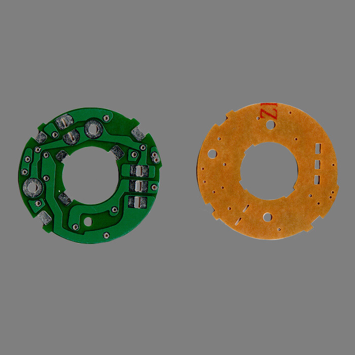
Commodity Name: Single Layer Printed Circuit Board for Medical
Place of Origin: Jiangsu, China
Brand Name: HFast
Base Material: Copper
Layers: 1L
Board Thickness: 1.60mm
Copper Thickness: 1oz
Minimum Hole Size: 0.8mm
Surface Treatment: OSP
Color: Green Oil and Black Legend
Advantages: CEM1 Material, Fire Resistance Grade: 94V-0
Brief Introduction of Single and Double Layer PCB
Single and double-layer PCB (single panel/double-sided board) is the most basic, economical, and widely used type of printed circuit board. They form the cornerstone of the electronics industry, especially suitable for low complexity and cost sensitive scenarios.
In today's era of high-end multilayer boards, single and double-layer boards are still the silent majority in the electronic world - they may not be stunning enough, but they support the stable operation of 80% of civilian electronic devices.
Characteristics of Single and Double Layer PCB
1. Low cost;
2. Simple manufacturing and short delivery time;
3. Easy to produce, maintain, and weld;
4. Suitable for simple circuits;
5. Low wiring density.
Core manufacturing process flow of Single and Double Layer PCB
1. Single panel process flow (simple and efficient)
A [cutting] -->B [drilling]
B -->C [Graphic Transfer]
C -->D [Etching]
D -->E [Solder mask printing]
E -->F [Character Printing]
F -->G [Surface Treatment]
G -->H [Forming Test]
Pain point : Unable to achieve cross wiring, requiring manual jumper (increasing failure rate).
2. Breakthrough in core process of dual panel (metalized holes)
A [cutting] -->B [drilling]
B -->C [Chemical Copper Deposition] -->D [Electroplating Thickening]
D -->E [outer graphic] -->F [etching]
F -->G [solder mask/character] -->H [surface treatment]
Technical key: Chemical deposition of copper deposits a conductive layer (0.3-1 μ m) on the hole wall, followed by electroplating of copper to thicken it to 20-25 μ m.
Design specifications of Single and Double Layer PCB
1. Single panel design follows the iron law
Jumper rule : Jumper spacing ≥ 2mm to avoid cross short circuits
-Line width/spacing: Conventional ≥ 0.3mm/0.3mm (low-cost process)
-Solder pad design: Diameter ≥ drilling+0.5mm, anti stripping
2. Optimization strategy for double-sided panels
Via design:
-Through hole diameter ≥ 0.3mm (8mil)
-Pad ring width ≥ 0.15mm (6mil)
-Wiring Techniques:
-Top level goes horizontally, bottom level goes vertically
-Key signals should be kept away from the edge of the board (≥ 1mm)
Core application scenarios and selection logic of Single and Double Layer PCB
1. Single panel absolute advantage field
-Consumer Electronics: Remote Control, Electronic Scale, Simple Toys
-Power module: LED driver power supply, charger control board
-Electrical Control: Washing Machine Timer, Fan Speed Control Board
Selection logic: Circuit nodes<50, no IC or only direct insertion IC
2. Applicable scenarios for double-sided panels
-Industrial Control: PLC I/O Module, Sensor Interface Board
-Automotive Electronics: Lamp Controller, Wiper Module
- Communication equipment: router power board, RF modulation board
Selection logic: Digital circuits that require dense wiring (MCU systems)
Technological Evolution and Alternative Boundaries of Single and Double Layer PCB
1. Single panel innovation direction
-Jumper Process Upgrade: Pre formed Jumper Frame (Consistency Improved by 40%)
-Thick Copper Application: 2 oz Copper Foil Power Board (3x Increase in Current Carrying Capacity)
-Substrate Expansion: Aluminum based single panel (LED heat dissipation requirements)
2. Breakthrough in double-sided panel technology
-Blind buried hole miniaturization: Laser drilling micro holes (0.1mm) for wearable devices
-High frequency material application: RO4350B mixed pressure plate (5G IoT terminal)
-Surface treatment upgrade: ENEPIG replaces tin spraying (improves solder joint reliability)
>Irreplaceability: In 2023, single/double-sided boards still accounted for 62% of global PCB production (Prismark data), due to their unparalleled cost-effectiveness.
Practice tip: The maximum density limit for dual panel wiring is 20cm/cm ² (line width/spacing=0.2mm/0.2mm), exceeding this density requires upgrading to a multi-layer board.
Online Message
Application


CONTACT US
Please use the form below to get in touch.
If you need a reply we will get in touch as soon as possible.