
PRODUCT
PRODUCT
CONTACT US
 Printed Circuit Board")
 Printed Circuit Board")
 Printed Circuit Board")
 Printed Circuit Board")
 Printed Circuit Board")
 Printed Circuit Board")
 Printed Circuit Board")
 Printed Circuit Board")
 Printed Circuit Board")
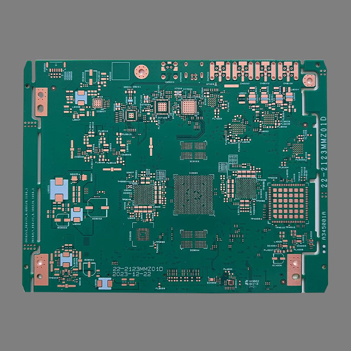
Commodity Name: Multi-layer HDI Printed Circuit Board For Vehicle SOC
Place of Origin: Jiangsu, China
Brand Name: HFast
Base Material: Copper or Aluminum
Layers: 10L
Board Thickness: 1.0mm
Minimum Hole Size: 0.10/0.20mm
Minimum Line Width: 0.076mm
Minimum Line Spacing: 0.076mm
Surface Treatment: Gold Plating
Color: Green Oil and White Legend
PCB Standard: IPC-A-600
Brief Introduction of High Density Interconnect PCB
HDI (High Density Interconnect) PCB board is a printed circuit board specifically designed to achieve higher wiring density. It accommodates more complex circuits in a smaller space by using finer line width/spacing, smaller via holes, higher pad density, and thinner core material.
HDI PCB is a key technology for modern electronic devices to achieve miniaturization, lightweight, and high performance. It achieves unprecedented interconnect density and electrical performance in a limited space by widely using micropores (blind holes, buried holes), fine circuits, thin materials, and layering processes. Despite high manufacturing costs and complex processes, it is an indispensable solution in fields such as smartphones, wearable devices, automotive electronics, medical equipment, and high-speed communication, and continues to evolve with the continuous development of electronic products (such as the mSAP/SAP process for finer lines and the popularization of arbitrary layer interconnects). Understanding HDI technology is crucial for designing compact, high-performance next-generation electronic products.
Characteristics of HDI PCB
1. Extremely high thermal conductivity;
2. Excellent insulation performance;
3. Thermal expansion coefficient matched with silicon;
4. High mechanical strength and rigidity;
5. Excellent chemical stability and corrosion resistance;
6. Good high-frequency performance;
7. High operating temperature;
8. Good dimensional stability;
9. Can achieve high-density wiring;
10. Low gas release.
Typical Application Areas of HDI PCB
*Smartphones and tablets: motherboards, camera modules, RF modules, etc.
Laptops and ultrabooks:motherboard, high-speed interface card.
*Wearable devices: smartwatches, wristbands, AR/VR devices.
Digital cameras and camcorders:Image sensor module, motherboard.
*Medical Electronics: Implantable devices, portable diagnostic devices, endoscopes.
*Automotive Electronics: Advanced driving assistance systems, infotainment systems, and body control modules (especially in confined spaces).
*Aerospace and Defense: Radar, Communication Systems, Guidance Systems (requiring miniaturization and high performance).
High performance computing:Cards that require high-speed interconnection in servers, switches, and routers.
*IoT devices: various miniaturized and intelligent sensor nodes and gateways.
Online Message
Application


CONTACT US
Please use the form below to get in touch.
If you need a reply we will get in touch as soon as possible.