
PRODUCT
PRODUCT
CONTACT US
")
")
")
")
")
Key Parameters of High Speed PCB
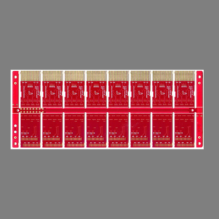
Commodity Name: High Speed Printed Circuit Board
Brand Name: HFast
Board Thickness: 1.00mm
Layers: 4L
Minimum Hole Size: 0.20mm
Minimum Line Width: 0.20mm
Minimum Line Spacing: 0.20mm
Surface Treatment: Gold Plating + 30U Gold-finished Golden Finger
Color: Green Oil and White Legend
Advantages: Optical module, speed of 48-96Gbps,Non lead gold finger electroplating with thick gold, gold finger chamfering, controlled depth step groove. Made with low DK and low DF materials.
Brief Introduction of High Speed PCB
High Speed PCB is designed specifically for transmitting high-frequency signals (usually>50MHz) and fast edge rates (<1ns), with the core goal of ensuring signal integrity (SI) and power integrity (PI). Its design difficulty far exceeds that of ordinary PCB, requiring collaborative solutions to complex issues such as impedance control, loss suppression, and crosstalk isolation.
High speed PCB is a fusion of signal integrity, material science, and precision manufacturing
-Cost trade-off: Ordinary FR-4 board costs $0.5/dm ², while Rogers RO4835 ™ Up to $30/dm ²;
-Performance boundary: The current technological limit is single channel 112Gbps (such as 800G optical modules), requiring mSAP technology to achieve a line width of 20 μ m;
-Future direction: Optoelectronic hybrid PCBs (silicon optical integration) and embedded passive devices (IPD technology) are breaking through traditional electrical bottlenecks.
>Designing high-speed PCBs is like riding an electromagnetic storm - every micrometer of error can trigger system crashes. Mastering the rules is the foundation of survival, understanding the essence is the key to breakthrough.
Characteristics of High Speed PCB
1. Ultra low signal loss;
2. Precise impedance control;
3. Optimization of electromagnetic compatibility(EMI);
4. Through hole optimization.
Four pillars of high-speed PCB design of High Speed PCB
1. Precise impedance control
-Calculation Model:
$$Z_0 = frac{87}{sqrt{varepsilon_r +1.41}}lnleft(frac{5.98H}{0.8W + T}right) quad text{( Microstrip Line)$$
Among them: H=dielectric thickness, W=line width, T=copper thickness, εᵣ=dielectric constant
-Tolerance requirement: ± 10% (USB4=85 Ω± 7%, PCIe 6.0=100 Ω± 5%)
-Implementation method:
-Select low deviation boards (such as Isola FR408HR with ε ᵣ=3.65 ± 0.05)
-Strictly control the etching factor (line width error < ± 8%)
2. Loss optimization technology
|* * Loss type * * | * * Suppression scheme * * | * * Effect * *|
|* * Conductor loss * * | Ultra low roughness copper foil (RTF ≤ 1.8 μ m, HVLP ≤ 1.2 μ m) | 10GHz loss reduced by 40%|
|* * Dielectric loss * * | Low Df board (Df<0.005, such as Rogers RO4350B) | 4 times better than FR-4 (Df ≈ 0.02)|
|* * Surface effect * * | Smooth solder mask ink (LPI type, roughness Ra<0.5 μ m) | Reduce skin effect loss above 30GHz|
3. Crosstalk and isolation design
-3W principle: Line spacing ≥ 3 times line width (e.g. 0.1mm line width, spacing ≥ 0.3mm)
-Grounding hole shielding: Differential grounding holes are installed on both sides at intervals of λ/10 (λ=signal wavelength)
-Cross division prohibition: High speed signal lines are strictly prohibited from crossing the power plane division gap.
4. Power Integrity (PI) Guarantee
-Target Impedance: $$Z_ {target}= frac { Delta V} { Delta I} quad text {Example: CPU core voltage requirement<1m Ω @ 100MHz-1GHz)}$$
-Implementation Plan:
-Low ESR decoupling capacitor array (MLCC+tantalum capacitor combination)
-Flat capacitor design (2mil dielectric layer, capacitance density>500nF/cm ²)
Special requirements for manufacturing processes of High Speed PCB
1. Over strict tolerance
-Line width tolerance: ± 0.015mm (ordinary board ± 0.05mm)
-Inter layer alignment: ± 0.025mm (HDI level accuracy)
2. Back Drilling Technology
-Remove unnecessary copper pillars (Stub) from through holes to reduce resonance (necessary for frequencies greater than 5GHz)
-Residual pile length control: $$L_ {stub}< frac { lambda} {10}= frac {c} {10f sqrt { varepsilon_r}} quad text {Example: 10GHz signal requires residual pile<1.2mm)}$$
3.Surface treatment optimization
|* * Process * * | * * Flatness * * | * * Applicable speed * * | * * Cost * *|
|ENEPIG * * | >56Gbps | High|
|* * Sinking Silver * * | < 25Gbps | Medium|OSP * * | <10Gbps | Low|
Design validation tool chain of High Speed PCB
1.Simulation analysis
-SI: ANSYS HFSS (3D Field Solution), Cadence Sigrity (Channel Analysis)
-PI: PowerSI (Power Network Impedance Simulation), Apache RedHawk (Chip Board Collaboration)
1. Testing methods
-TDR (Time Domain Reflectometer): Impedance Continuity Detection (Resolution ± 0.5 Ω)
-VNA (Vector Network Analyzer): S-parameter measurement (>40GHz bandwidth)
Online Message
Application


CONTACT US
Please use the form below to get in touch.
If you need a reply we will get in touch as soon as possible.