
PRODUCT
PRODUCT
CONTACT US
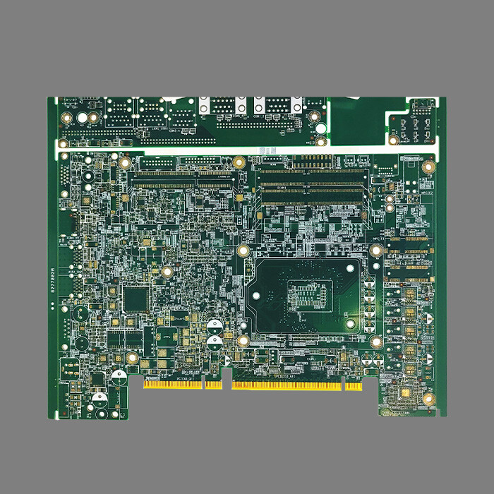


Commodity Name: Golden Finger Printed Circuit Board for Communication
Brand Name: HFast
Layers: 8L
Board Thickness: 1.60mm
Minimum Hole Size: 0.20mm
Minimum Line Width: 0.10mm
Minimum Line Spacing: 0.10mm
Surface Treatment: Lead free tin spraying+gold finger plating
Color: Green Oil and White Legend
Advantages: Golden finger chamfering adopts CNC internal inclination and Gold Finger Cover with High Temperature Tape and Spray Tin
Brief Introduction of Golden Finger PCB
The golden finger PCB board is a gold-plated conductive contact on the edge of the circuit board, which is electrically connected to other devices by inserting it into a slot. Its surface is composed of numerous golden touch pads, named after its finger like shape, mainly used for signal transmission between hardware such as memory modules, graphics cards, and motherboards.
Core functions of Golden Finger PCB
The gold finger transmits data and current through conductive contacts, for example, all data and electronic streams of the memory processing unit are exchanged with the motherboard through the gold finger. Its gold plating layer has high conductivity, wear resistance, and oxidation resistance, which can reduce contact resistance and protect internal circuits.
Manufacturing Process of Golden Finger PCB
Using electroplating technology to cover a gold layer on copper-clad laminates (usually only a few tens of micrometers thick), common processes include:
Electroplated hard gold: The coating has high hardness and is suitable for frequent insertion and removal scenarios, but the cost is relatively high.
Chemical gold plating (ENIG): High cost-effectiveness, but good soldering performance, suitable for non high frequency insertion and extraction scenarios.
Design Points of Golden Finger PCB
Oblique edge treatment: It is usually designed with a 45 degree beveled edge to avoid damaging the board edge during insertion and removal.
Solder mask treatment: The gold finger area needs to have a window design to avoid solder mask ink falling off and affecting contact.
Chamfering design: Chamfering the contour line can improve the smoothness of insertion and removal, and reduce stress concentration.
Online Message
Application


CONTACT US
Please use the form below to get in touch.
If you need a reply we will get in touch as soon as possible.