
PRODUCT
PRODUCT
CONTACT US
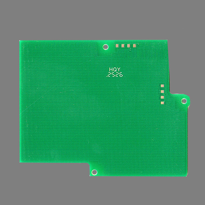
Commodity Name: Circuit Printed Circuit Board for POS Machine
Brand Name: HFast
Layers: 2L
Board Thickness: 1.00mm
Minimum Hole Size: 0.25mm
Minimum Line Width: 0.127mm
Minimum Line Spacing: 0.127mm
Surface Treatment: Gold Plating
Color: Green Oil and White Legend
Brief Introduction of Circuit PCB
The term 'circuit PCB board' is not a standard term, but it clearly points to the core function of printed circuit boards: providing a support platform for electronic components and interconnecting electrical 'circuits'
Core concept of Circuit PCB
*Circuit: In electronics, "circuit" refers to the path through which current can form a complete path. Without a closed circuit, current cannot flow and electronic devices cannot function.
*PCB: Printed Circuit Board.
*Circuit PCB board=PCB that realizes electrical connections: Therefore, "circuit PCB board" refers to the substrate that carries electronic components and connects them through its internal conductive paths (wiring) to form a working current circuit.
The essence of PCB is to build a "circuit":
*The core value of PCB lies in its use of copper foil to etch pre designed wires (traces) and solder pads on insulating substrates (such as FR4).
*These copper foil wires are the current channels that precisely connect the pins of various components.
*After the components (resistors, capacitors, chips, etc.) are soldered onto the solder pads of the PCB, their electrical connections are completed through these copper foil traces, thus forming complete electrical circuits required for various functions.
*Without these carefully designed "circuits" (wiring), PCB is just an insulating board without electrical functions.
How to implement the "circuit" function on PCB
** * Design: * * Engineers use EDA software to design PCB layouts based on circuit schematics, determining the positions of components and the copper foil routing paths connecting them. This is in the process of designing a circuit.
** * Manufacturing:**
** * Substrate: * * Provides insulation support.
*Copper coating: Copper foil is pressed onto both sides or inner layers of the substrate.
** * Graphic transfer: * * Transfer the designed wiring pattern onto a copper-clad laminate through photolithography process.
*Etching: Use chemical solution to etch away unwanted copper foil, leaving only the designed wires (traces/circuits) and solder pads.
*Drilling: Drilling installation holes, positioning holes, and through holes for connecting wires of different layers.
*Hole metallization: Plating metal (usually copper) on the inner wall of the via to achieve vertical connections between different conductive layers, forming a three-dimensional circuit.
*Solder mask: Apply green oil (or other colors) to non welding areas to prevent short circuits and oxidation.
*Screen printing layer: Printing auxiliary information such as component part numbers and polarity markings.
** * Final product: * * A bare board with a predetermined "circuit" (copper foil routing network) waiting to be assembled into a PCBA.
Types of PCBs and "circuit" complexity
*Single panel: All circuits (wiring) are completed on one side. The simplest, lowest cost, suitable for simple circuits.
*Double sided board: The circuit (wiring) is distributed on both sides, and the wiring on both sides is connected through via holes. This is the most common type, suitable for circuits of moderate complexity.
*Multi layer board: It is composed of 4 or more layers of conductive copper foil and insulation laminate. The internal copper layer (inner layer) is usually used as a power layer or geological layer, while the outer layer is used for signal lines. Connect each layer through vias. Used for high-density, high-speed, and high complexity circuits (such as mobile phone motherboards and computer motherboards). Multilayer boards construct an extremely complex three-dimensional circuit network, which is the core of modern electronic devices.
The relationship between circuit PCB board (PCB) and PCBA:
*PCB is the foundation that provides a physical installation platform and a pre-set electrical connection "circuit" skeleton.
*PCBA is a finished product, which is the state after the components are correctly installed and soldered onto the PCB. At this point, the preset "circuit" skeleton is activated by the components, forming a truly functional electronic circuit.
Online Message
Application


CONTACT US
Please use the form below to get in touch.
If you need a reply we will get in touch as soon as possible.