
PRODUCT
PRODUCT
CONTACT US


Key Parameters of High Frequency PCB
Commodity Name: High Frequency Printed Circuit Board
Brand Name: HFast
Material:
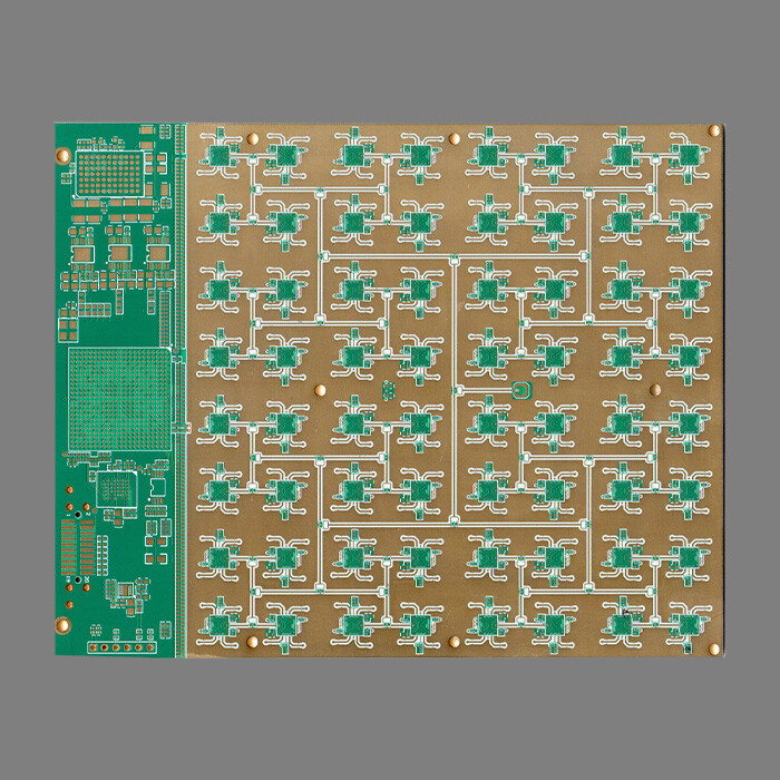
Layers: 6L
Range of Copper Thickness: 2-9oz
Density: 3.7g/cm3
Flexural Strength: 466-496Mpa
Surface Roughness: 0.3-0.5
Thermal Conductivity: >170
Dielectric Strength: >15KV/mm
Dielectric Constant: 9.0Mhz
Brief Introduction of High Frequency PCB
High Frequency PCB is designed specifically for RF and microwave circuits (usually>1GHz), with the core goal of minimizing signal loss and maintaining phase stability. It is widely used in fields such as 5G communication, radar, and satellite systems. The core of its technology lies in low loss dielectric materials and precise electromagnetic field control.
High frequency PCB is the ultimate fusion of materials science and electromagnetic field engineering
-Cost Limit: The unit price of PTFE sheet is over $500/m ², while FR-4 is only $10/m ². Hybrid lamination (high-frequency layer+FR-4 support layer) is a compromise solution;
-Performance limit: The loss of existing materials increases dramatically above 110GHz, and * * Gallium Nitride (GaN) substrate * * and * * Terahertz LCP * * are breakthrough directions;
-Integration Trend: AiP (Antenna Integrated Packaging) technology integrates RF front-end with PCB to shorten path loss (such as Apple millimeter wave antenna module).
Characteristics of High Frequency PCB
1. Ultra low signal loss;
2. Precise impedance control;
3. Optimization of electromagnetic compatibility(EMI);
4. Through hole optimization.
Special requirements for manufacturing processes of High Frequency PCB
1. Precision graphic transfer
-Laser direct imaging (LDI): Line width tolerance ± 0.01mm (ordinary exposure ± 0.05mm)
-Vacuum etching: Side etching control<15% to ensure impedance consistency
2. Laminated process
-Low pressure compression (<200psi) prevents deformation of PTFE material
-Heating rate<2 ℃/min to avoid substrate delamination
1. Surface treatment
|* * Process * * | Flatness | High frequency applicability | Disadvantages|
|ENEPIG * * | Ultra high frequency (>60GHz) | High cost|
|* * Sinking Silver * * | < 20GHz | Easily corroded by sulfides|
|OSP * * | < 5GHz | Poor soldering resistance|
Verification and testing methods of High Frequency PCB
1. Vector Network Analyzer (VNA)
-Measure S parameters (S11 return loss<-20dB, S21 insertion loss<0.1dB/cm)
-Time domain reflectometry (TDR) detects impedance continuity (resolution ± 0.5 Ω)
2. Dielectric performance testing
-Resonant cavity method: Accurate measurement of Dk/Df (error<± 2%)
-SPDR method: wideband sweep (1-110GHz)
Online Message
Application


CONTACT US
Please use the form below to get in touch.
If you need a reply we will get in touch as soon as possible.