
PRODUCT
PRODUCT
CONTACT US
")
")
")
")
")
Key Parameters of Thick Copper PCB
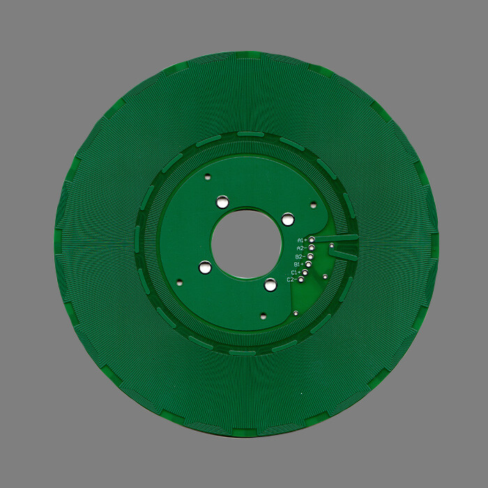
Commodity Name: Thick Copper Printed Circuit Board for Vehicle Power Management
Brand Name: HFast
Base Material: Copper
Layers: 4L
Board Thickness: 2.00mm
Minimum Hole Size: 0.40mm
Minimum Line Width: 0.25mm
Minimum Line Spacing: 0.25mm
Surface Treatment: Immersion Tin
Color: Green Oil and White Legend
Advantages: Designed for Automotive power management and resistant to high current load
Brief Introduction of Heavy Copper PCB
Thick copper PCB also called Heavy Copper PCB, refers to a circuit board that uses copper foil with a thickness of ≥ 3oz (105 μ m) on the outer or inner layer. The ultra-high power version can reach 20oz (700 μ m) or more. Its core value lies in carrying a hundred ampere level current, efficient thermal conductivity, and structural reinforcement. It is the cornerstone technology for high-voltage and high current scenarios such as new energy, industrial power, and rail transit.
The essence of choosing thick copper PCB is to choose "zero current compromise" - when electronic systems enter the kilo-ampere era, the thickness of copper is the moat for energy passage.
Evolution of Three Layer Structure of Thick Copper PCB
1. Standard symmetrical structure (3-10oz)
|* * Sequence * * | * * Materials and Processes * * | * * Key Parameters * *|
|Signal layer | Rolled copper (low roughness Ra<1.8 μ m) | Line width/spacing ≥ 0.3mm|
|Insulation layer | High Tg FR-4 (>180 ℃) or polyimide | Voltage resistance>3kV/mm|
|Inner layer copper thickness | Symmetrical design (such as 2-4-2: outer layer 2oz/inner layer 4oz) | Avoid lamination warping|
2. Ultra thick copper mixed structure (12-20oz)
-Gradient copper thickness design:
`Power zone 20oz → transition zone 10oz → signal zone 3oz`
-Embedded copper block:
① Milling grooves inside the board → ② Pressing copper blocks → ③ Electroplating leveling (current carrying ↑ 50%)
Breakthrough in key manufacturing processes of Heavy Copper PCB
1. Graphic Transfer Technology
|* * Challenge * * | * * Traditional process defects * * | * * Thick copper solution * * | * * Effect * *|
|Severe lateral corrosion | Line width loss>50% | Differential etching+pulse plating | Loss<15%|
|Copper plated voids | Uneven copper thickness in high aspect ratio holes | Vibration electroplating+organic additives | Uniformity>90%|
|* * Laminated delamination * * | Insufficient resin flow | Vacuum lamination (>300psi)+semi cured sheet pre drying | Zero delamination defects|
2. Special drilling and surface treatment
-Deep hole drilling technology:
-Drill bit aspect ratio ≤ 15:1 (Example: A 3mm thick plate requires a Φ 0.2mm drill bit)
-Segmented cutting (0.05mm chip removal per drill)
Preferred surface treatment:
|* * Craftsmanship * * | Applicable Scenarios | Performance Advantages|
|Chemical nickel palladium plating |>10A signal pin | Flatness ± 0.5 μ m, corrosion-resistant|
|Selective silver plating | Power busbar | Electrical resistivity 1.6 μ Ω· cm, current carrying ↑ 30%|
|Antioxidant OSP | Short term storage | Cost reduction of 40%, excellent solder resistance|
The Golden Rule of Design of Heavy Copper PCB
1. Current carrying calculation model
$$I = K cdot Delta T^{0.44} cdot A^{0.725}$$
-K : Material constant (copper=0.048)
-Δ T : Allowable temperature rise (℃)
-A : Copper cross-sectional area (mil ²)
► Example: 6oz copper (210 μ m) × 10mm line width →cross-sectional area A=84000 mil ² → Δ T=20 ℃ current carrying ≈ 280A
2. Design Specification for Via Holes
|* * Parameter * * | * * Standard Value * * | * * Risk Avoidance * *|
|Aperture/copper thickness ratio | ≥ 1:1 | Φ 0.3mm hole requires ring width ≥ 0.3mm|
|Number of current carrying holes | N ≥ I/2A (A=single hole current carrying capacity) | Example: 100A requires 8 Φ 0.5mm through holes|
|Hot via array | Φ 0.3mm holes @ 1mm spacing | filled with thermal conductive epoxy resin (>5W/m · K)|
3. Heat dissipation enhancement strategy
-Copper layer topology optimization:
! [Schematic diagram of thermal topology optimization]( https://via.placeholder.com/300x150?text=Thermal +Spreading+Design)
-Direct heat dissipation path: Design below the power device Solid copper area ≥ 3 times the device area → Combined with thermal conductive silicone grease directly connected to the shell
Technological Evolution Direction of Heavy Copper PCB
1. Nano crystalline copper foil
-Grain size<100nm → conductivity increased by 15% (RRR>500) → used for superconducting interconnects in quantum computers
2. 3D printed circuit
-SLM technology manufacturing curved thick copper structure → wall thickness accuracy ± 0.1mm → adaptable to irregular motor controller
3. Hybrid cooling system
-Etching of copper layer microchannel(width 200 μ m) → Water cooling thermal resistance reduced to 0.02 ℃/W
2. Ultra high speed electroplating
-Pulse reverse electroplating (50 μ m/min) → achieving * * 40oz (1.4mm) * * copper layer without voids
Online Message
Application


CONTACT US
Please use the form below to get in touch.
If you need a reply we will get in touch as soon as possible.