
PRODUCT
PRODUCT
CONTACT US
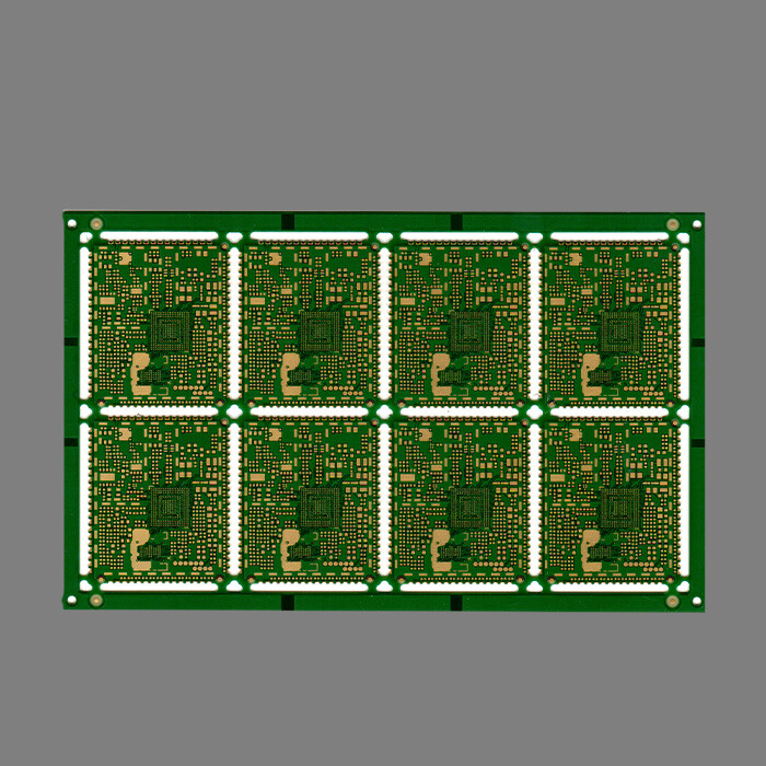


Key Parameters of Semi Hole PCB
Commodity Name: Semi Hole Circuit Board for Communication
Brand Name: HFast
Base Material: Copper
Layers: 12L
Board Thickness: 1.20mm
Minimum Hole Size: 0.20mm
Minimum Line Width: 0.076mm
Minimum Line Spacing: 0.076mm
Surface Treatment: Immersion Gold
Color: Green Oil and White Legend
Brief Introduction of Semi Hole PCB
Half hole PCB (Castellated Holes PCB) is a special circuit board designed for modular splicing, board to board vertical assembly, or surface mount (SMT) by processing metalized half holes * * at the edge of the board. Its core value lies in eliminating connectors, improving space utilization, and enhancing high-frequency performance. It is widely used in compact devices such as IoT modules, smart wearables, and communication gateways.
Half hole PCB is the core carrier for miniaturization and modularization of electronic systems - by converting "connectors" into "onboard structures".
The essence of choosing a half hole PCB is to choose the ultimate simplification of connections - as electronic devices move towards the molecular scale, the half hole structure becomes a metal bridge that crosses the microscopic world.
The core advantages and principles of Half Hole PCB
|* * Features * * | * * Half hole PCB * * | * * Traditional connector solution * * | * * Improved effect * *|
|* * Space occupation * * | Board edge directly welded, thickness ≤ * * 0.8mm * * | Connector height>2.5mm | * * Save 70% vertical space * *|
|* * Signal integrity * * | Direct connection without contact, continuous impedance | Connector impedance mutation ± 20% | High speed signal jitter reduction * * 50% * *|
|* * Assembly cost * * | Eliminating connectors+SMT to complete in one go | Additional plugins+welding process | BOM cost reduced by * * 40% * *|
|* * Reliability * * | Solder joint mechanical strength>* * 50N * * | Connector insertion and extraction force<30N | Anti vibration improvement * * 300% * *|
Working principle :
>By controlling deep milling, the through-hole is cut along the edge of the plate, and the hole wall is metalized to form a weldable semi cylindrical surface, achieving:
Module stacking: Align the upper and lower half holes and reflow solder paste to form a three-dimensional circuit;
Edge Welding: Directly attached to the motherboard solder pad, replacing gold fingers.
Structural types of Castellated Holes
1. Standard half hole (single-sided)
|* * Parameters * * | * * Specifications * * | * * Applicable Scenarios * *|
|* * Aperture * * | 0.6~1.2mm | Power/Ground Pin|
|* * Hole spacing * * | 1.0~2.0mm | Signal transmission pin|
|* * protrusion amount * * | 0.1~0.3mm (extension outside the board) | enhanced solder joint strength|
2. Staggered half hole (bilateral)
-Structure: Half holes on both sides of the board are arranged in a staggered manner (to avoid welding short circuits)
-Advantages: 2x increase in I/O density (suitable for multi-channel sensor modules)
-Limitations: Requires double-sided SMT process
3. Step half hole composite structure
-Combined with step PCB technology: Half hole is located in the step area to reduce the thin layer (thickness 0.6mm → reduced to 0.3mm)
-Application: Ultra thin folding device hinge circuit (such as OPPO Find N3)
Key Manufacturing Processes and Challenges of Half Hole PCB
1. Half hole forming process**
|* * Steps * * | * * Process Points * * | * * Accuracy Requirements * *|
|* * Drilling * * | Mechanical drilling through hole (aperture tolerance ± 0.05mm) | Position deviation < ± 0.1mm|
|* * Hole metallization * * | Chemical deposition of copper+electroplating of copper (hole wall thickness ≥ 25 μ m) | Copper thickness uniformity>90%|
|* * Shape milling * * | Hard alloy milling cutter cuts along the center of the hole (speed 30000 rpm) | Half circle deviation < ± 0.03mm|
|* * Deburring * * | Plasma etching (RF power 500W) | Surface roughness Ra<1.6 μ m|
1. Core Difficulty Solution
|* * Difficult problem * * | * * Failure risk * * | * * Innovative process * *|
|------------------|------------------------|-----------------------------|
|* * Copper wall tearing * * | Half hole edge copper foil curling | * * Laser micro melting reinforcement * *: 1064nm fiber laser local annealing|
|Insufficient solder climb * * | virtual soldering | * * chemical micro roughening * *: ammonium nitrate micro etching increases bonding strength|
|* * Resin residue at the edge of the board * * | Solder mask ink covering the solder pad | * * LDI precise exposure * *: Solder mask window accuracy ± 10 μ m|
The Golden Rule of Design of Half Hole PCB
1. Half hole layout specification
-Safety distance:
-The distance between the center of the half hole and the edge of the plate is ≥ 0.5 times the diameter of the hole (for example, a diameter of 1mm hole needs to be ≥ 0.5mm from the edge)
-The center distance between half holes is ≥ 2 times the diameter of the hole (anti bridging)
-Pad strengthening:
-Add * * stolen solder pads * * (size 0.3 × 0.5mm) around the half hole to absorb excess solder
2. Key points of electrical design
-Impedance Control:
Half hole area line width adjustment formula:
$$W_{adj} = W cdot frac{varepsilon_{r_new}}{varepsilon_{r_base}} cdot sqrt{frac{H_{base}}{H_{adj}}}$$
(W=original line width, H=dielectric thickness, εᵣ=dielectric constant)
-Current carrying capacity:
Half hole current carrying capacity ≈ 60% of the same diameter through-hole (additional parallel holes are required)
3. SMT assembly requirements
|* * Parameter * * | * * Recommended Value * * | * * Critical Risk * *|
|* * Solder paste thickness * * | 0.12~0.15mm |<0.10mm (virtual soldering)|
|* * Reflux peak * * | 245 ± 5 ℃ (SnAgCu solder) |>260 ℃ (copper layer oxidation)|
|* * Mounting pressure * * | 1~2N/half hole |>3N (damaged half hole structure)|
Technological Evolution Direction of Semi Hole PCB
1. Laser micro hole half hole
-UV laser processing of Φ 0.1mm micro half holes with a spacing of 0.2mm (suitable for 100G optical modules)
2. Vertical conductive adhesive
-Fill the half hole with anisotropic conductive adhesive (ACP) to achieve low-temperature pressure bonding (<150 ℃)
3. 3D stacking optimization
-Half hole+through silicon via (TSV) hybrid interconnect with interlayer delay<0.5ps
4. Intelligent detection system
-AOI+3D confocal scanning, real-time monitoring of half hole solder climb height (accuracy ± 5 μ m).
Online Message
Application


CONTACT US
Please use the form below to get in touch.
If you need a reply we will get in touch as soon as possible.