
PRODUCT
PRODUCT
CONTACT US
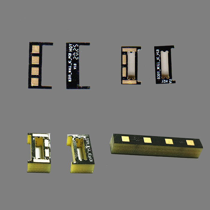


Commodity Name: Mini Wall-mounted Printed Circuit Board for POS Machine
Brand Name: HFast
Layers: 4L
Board Thickness: 3.0-4.0mm
Minimum Hole Size: 0.40mm
Minimum Line Width: 0.127mm
Minimum Line Spacing: 0.127mm
Surface Treatment: Gold Plating
Color: Black Oil and White Legend
Advantages: Thickness exceeds the standard and circuit board
Brief Introduction of Miniature Wall-mounted PCB
Miniature Printed Circuit Board refers to a printed circuit board that is very small in size, compact in structure, and has high-density interconnect characteristics. They are key foundational components for the miniaturization, portability, and high performance of modern electronic devices.
Mini PCB board is the cornerstone of the development of modern electronic technology towards miniaturization and high performance. It utilizes advanced technologies such as HDI to achieve complex circuit interconnection and functional integration in extremely limited space. Despite facing challenges such as complex design, high manufacturing costs, and difficult heat dissipation, its applications in fields such as smartphones, wearable devices, medical electronics, and the Internet of Things are indispensable, continuously pushing the boundaries of innovation in electronic products. Choosing and using mini PCBs requires a careful balance between high performance, small size, reliability, and cost.
Core definition and characteristics of Mini Wall-mounted PCB
Small size: This is the most prominent feature. There is no absolute standard, but it usually refers to sizes much smaller than traditional PCBs, ranging from a few millimeters square (such as chip level packaging) to several centimeters square (such as small sensor modules, microcontroller boards).
*High density: Integrating a large number of components (resistors, capacitors, IC chips, connectors, etc.) and complex wiring in a limited space. This requires very fine line width/spacing.
Compact structure:Usually adopts multi-layer design (4 layers, 6 layers, 8 layers or even more), utilizing Z-axis space for wiring and maximizing the use of limited planar area.
*Precision Manufacturing: The manufacturing process requires extremely high precision exposure, etching, drilling (micro holes, blind buried holes), lamination, and surface treatment techniques.
Diverse types: can be hard board, flexible board (FPC), or rigid flexible combination board. Flexible boards are particularly important in scenarios where space is limited and there is a need for bending, such as wearable devices and camera modules.
Key technologies and processes of Mini Wall-mounted PCB
*HDI technology is the core of manufacturing mini PCBs. It uses finer line width/spacing (<100 µ m), smaller via holes (<150 µ m), micro holes (laser drilling), as well as blind and buried hole technologies to significantly increase wiring density.
*Micro pores: Laser drilling is used to form extremely small diameter holes (usually<150 µ m) that connect adjacent layers and save space.
*Blind/Buried Holes: Holes that only penetrate a portion of the board layer and do not penetrate the entire board, freeing up more surface and internal space for wiring and component placement.
** * Fine lines/spacing: * * Etch out wires with widths and spacing at the micrometer level.
*Advanced packaging: It is often used in combination with miniaturization packaging technologies such as CSP, WLCSP, SiP, etc.
*SMT: High precision surface mount technology used for precise soldering of small components (such as 0201, 01005 size resistors and capacitors, micro BGA chips) on small areas.
Main application areas of Mini Wall-mounted PCB
Portable and wearable devices: Smartphones, smartwatches, wireless headphones, fitness trackers, AR/VR glasses.
*Medical Electronics: Implantable devices (pacemakers, neurostimulators), endoscopes, portable monitors, disposable diagnostic sensors.
*Internet of Things: * * Small sensor nodes, RFID tags, smart home controller modules.
*Consumer Electronics: * * Miniature camera module, compact remote control, small gaming peripherals.
*Aerospace and Defense: Unmanned Aerial Vehicle Flight Control Board, Micro Navigation System, Electronic Module for Individual Soldier Equipment.
*Industrial control: * * Small PLC modules, compact sensors, micro actuator controllers.
*Automotive Electronics: * * Small ECU module, tire pressure monitoring sensor, in car camera module.
Advantages of Mini Wall-mounted PCB
** * Ultimate miniaturization: * * makes devices lighter, thinner, and more portable.
*Reducing weight is crucial for aviation, aerospace, and wearable devices.
** * Improve performance: * * High density cabling can shorten signal paths, reduce latency and interference, and enhance signal integrity (especially for high-frequency signals).
** * Increase functional density: * * Achieve complex functions in small spaces.
** * Reduce power consumption: * * Shorter interconnects typically mean lower resistance and power consumption (to some extent).
*Design flexibility: Especially for flexible PCBs, they can adapt to non planar spaces.
Challenges and considerations of Mini Wall-mounted PCB
*High design complexity: requires professional EDA tools and engineers, with extremely high requirements for layout and wiring, signal integrity, power integrity, and thermal management.
*High manufacturing costs: Precise processes, special materials, and lower yield rates (especially in the early stages) result in significantly higher costs than ordinary PCBs.
** * Manufacturing difficulty is high: The requirements for equipment accuracy, material stability, and process control are extremely demanding.
*Difficulty in heat dissipation: Small space, dense components, and difficulty in dissipating heat make thermal management a key challenge.
*Difficulty in testing and maintenance: Due to limited space, it is difficult to place testing points, and fault location and maintenance are extremely challenging, usually requiring specialized equipment.
*Material selection: Special substrate materials with high frequency, high thermal conductivity, and high reliability may be required, which increases costs.
** * Reliability requirements:Small devices may face more stringent environments (such as vibration, shock, temperature changes), which require higher mechanical and electrical reliability for PCB.
Online Message
Application


CONTACT US
Please use the form below to get in touch.
If you need a reply we will get in touch as soon as possible.