
PRODUCT
PRODUCT
CONTACT US
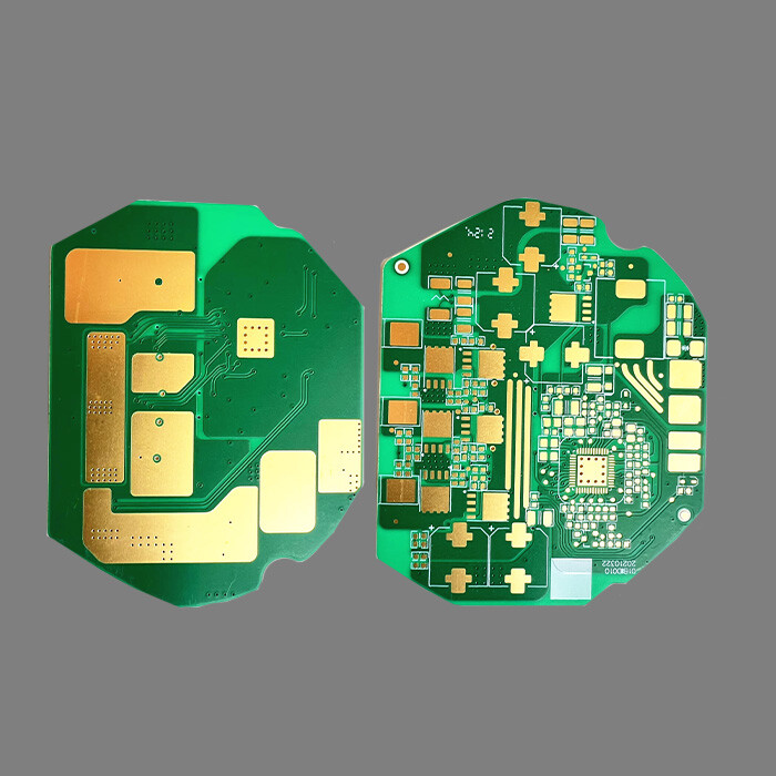


Key Parameters of DBC PCB
Commodity Name: Direct Bond Copper Printed Circuit Board
Brand Name: HFast
Type: DBC Metallized Ceramic Substrate
Material: Alumina Ceramic/Copper//Al2O2/AIN
Layers: 6L
Range of Copper Thickness: 2-9oz
Density: 3.7g/cm3
Flexural Strength: 466-496Mpa
Surface Roughness: 0.3-0.5
Thermal Conductivity: >170
Dielectric Strength: >15KV/mm
Dielectric Constant: 9.0Mhz
Brief Introduction of DBC PCB
Ceramic PCB is a circuit board made of ceramic materials such as aluminum oxide (Al 2O3), aluminum nitride (AlN), or beryllium oxide (BeO), which cannot be replaced in extreme high temperature, high frequency, and high insulation scenarios. Its core value lies in ultra-high thermal conductivity, near zero thermal expansion, and excellent chemical stability, widely used in cutting-edge fields such as aerospace, military, and RF power devices.
Ceramic PCB is the ultimate armor for extreme environmental electronic systems - when FR-4 carbonizes at 300 ℃ and metal substrates break down at kilovolts, only ceramics can conquer the triple hell of heat, electricity, and chemistry simultaneously.
The essence of choosing ceramic PCB is to break through the physical limits - at the forefront of human technology, ceramic substrates hold the hope of controllable nuclear fusion, deep space exploration, and life electronics.
Characteristics of Ceramic PCB
1. Extremely high thermal conductivity;
2. Excellent insulation performance;
3. Thermal expansion coefficient matched with silicon;
4. High mechanical strength and rigidity;
5. Excellent chemical stability and corrosion resistance;
6. Good high-frequency performance;
7. High operating temperature;
8. Good dimensional stability;
9. Can achieve high-density wiring;
10. Low gas release.
The Four Major Manufacturing Processes of DBC PCB
1. Thick Film Technology
-Process: Screen printing tungsten/molybdenum manganese paste → 1600 ℃ hydrogen sintering → Nickel gold plating
-Line width: ≥ 150 μ m
-Applicable: Automotive sensors, heating plates (low cost)
2. Thin Film Technology
-Process: Vacuum Sputtering of Titanium/Copper → Photolithography → Etching (Accuracy ± 1 μ m)
-Line width: 10~50 μ m
-Applicable: Microwave integrated circuits (such as radar T/R modules)
3. DPC (Direct Copper Plating)
-* * Process * *: Laser drilling → Magnetron sputtering of titanium/copper seed layer → Electroplating and hole filling
-Advantages: Strong vertical interconnection capability (depth to diameter ratio 1:1)
-* * Applicable * *: High density LED packaging, laser
4. HTCC/LTCC (High/Low Temperature Co fired Ceramics)
|* * Parameters * * | * * HTCC * * | * * LTCC * *|
|* * Sintering temperature * * | 1600~1800 ℃ (alumina) | 850~900 ℃ (glass ceramic)|
|* * Metal conductor * * | Tungsten/Molybdenum (high resistivity) | Silver/Gold (low resistivity)|
|* * Layers * * | ≤ 100 Layers | ≤ 20 Layers|
|* * Application * * | Aerospace high-temperature resistant module | Mobile RF module (BAW filter)|
Key process challenges and solutions of Ceramic Printed Circuit Board
1. Bonding force of metallization layer
-Problem: Ceramic metal thermal expansion mismatch leading to delamination
-Plan:
-Active brazing (Ag Cu Ti alloy, bonding strength>200MPa)
-Magnetron sputtered titanium/chromium transition layer (thickness 0.1~0.5 μ m)
2. Precision drilling
-Laser Micro hole: UV laser (355nm) drilling, aperture ± 5 μ m (Example: AlN plate drilling Φ 50 μ m hole)
-Grinding wheel cutting: Diamond grinding wheel (particle size ≤ 10 μ m) cutting, edge breakage<20 μ m
3. Co firing shrinkage control
-HTCC: Adding magnesium oxide/silicon oxide to adjust shrinkage rate (± 0.1% accuracy)
-LTCC: Pre sintered ceramic strip (shrinkage rate matched to ± 0.3%)
The Golden Rule of Design of Ceramic Printed Circuit Board
1. Thermal stress relief
-Align the power chip in the center to avoid eccentric thermal expansion;
-Four corner screw fixation (torque ≤ 0.6Nm), with indium foil buffer layer added.
2. High frequency wiring
-Coplanar waveguide (GCPW) replaces microstrip lines to reduce dielectric losses;
-The spacing between grounding holes is ≤ λ/10 (λ=wavelength in the medium).
3. High voltage insulation
-The electrode edge is designed with rounded corners (R>0.3mm) to suppress electric field concentration;
-Creepage distance>3mm/kV (doubled in humid environments).
Technological breakthrough direction of DBC PCB
1. Nano composite ceramics
-Graphene reinforced AlN (thermal conductivity>400W/(m · K)), with a thermal expansion coefficient approaching that of silicon (4.1ppm/℃)
2. Low temperature co fired metal
-Copper paste LTCC (sintering temperature 900 ℃), resistivity reduced to 2 μ Ω· cm (original silver paste 1.6 μ Ω· cm)
3. Additive Manufacturing
-Laser Selective Sintering (SLS) forming complex 3D ceramic circuits with an accuracy of ± 10 μ m
4. No beryllium substitution
-Boron nitride nanotube (BNNT) composite material (thermal conductivity 200W/(m·K), non-toxic)
Online Message
Application


CONTACT US
Please use the form below to get in touch.
If you need a reply we will get in touch as soon as possible.