
PRODUCT
PRODUCT
CONTACT US
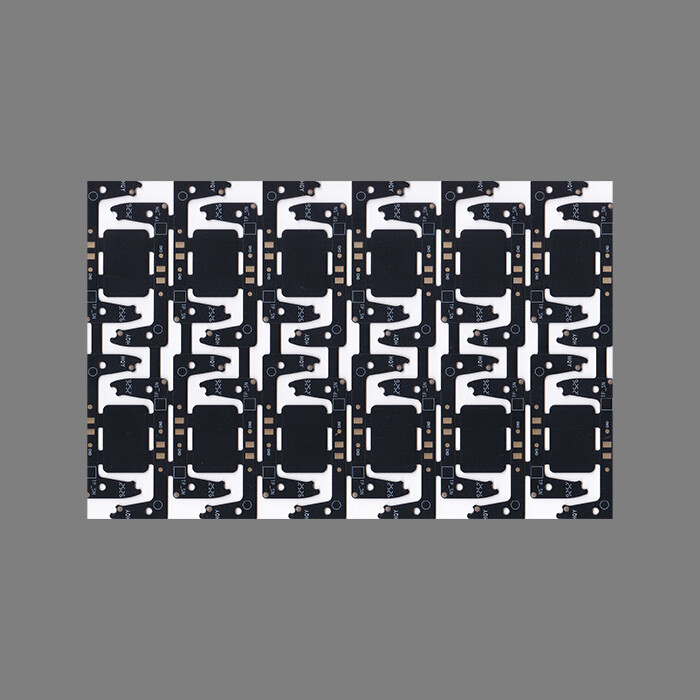

Commodity Name: Super Thin Printed Circuit Board for Communication with Double Sides
Brand Name: HFast
Layers: 2L
Board Thickness: 0.30mm
Minimum Hole Size: 0.25mm
Minimum Line Width: 0.15mm
Minimum Line Spacing: 0.15mm
Surface Treatment: Gold Plating
Color: Black Oil and White Legend
Brief Introduction of Super Thin PCB
Thin PCB board is relative to standard thickness (usually 1.6mm) and thick board, pursuing lightweight, miniaturization, flexibility (some types), and high-density interconnection.
Thin PCB board is one of the core technologies for achieving miniaturization, lightweighting, and portability of electronic devices, and is indispensable in fields such as consumer electronics, wearable devices, advanced packaging, and flexible electronics. However, its design and manufacturing face many challenges, with the core being to overcome the warping, deformation, and vulnerability caused by low rigidity.
Thin plates are a reflection of the electronic industry's pursuit of ultimate size and performance, with relatively high technical barriers and values.
Definition and Scope of Super Thin PCB
1. * * Thickness range:**
*Standard reference: The most common standard PCB thickness is 1.6mm.
*Definition of Thin Plate: PCB with a thickness of ≤ 1.0mm can be classified as "thin plate". In practical applications, the thickness range of thin plates is very wide:
*Ultra thin board: 0.4mm or thinner (such as 0.2mm, 0.3mm).
** * Conventional thin plate: * * 0.4mm -1.0mm (such as 0.6mm, 0.8mm).
*Relative concept: "Thin" is also relative. For PCBs with many layers (such as 12 or more), even if the total thickness is 1.2mm or 1.0mm, the single-layer dielectric thickness may be very thin, and the overall PCB belongs to the category of thin plates. Sometimes it also refers to the fact that the core board itself is very thin.
2. * * Core materials:**
*FR-4 and its variants: FR-4 is still mainstream, but high-quality materials suitable for thin plate processing need to be selected, such as FR-4 with high Tg, low CTE (coefficient of thermal expansion), and good dimensional stability. Ultra thin boards require extremely high material uniformity.
*Polyimide: Widely used in flexible PCBs and rigid flex PCBs, it has excellent flexibility, high temperature resistance, and dimensional stability, and is a key material for achieving ultra-thin and bendable properties.
** * Other special materials: * * such as LCP (liquid crystal polymer) for high-frequency ultra-thin applications, BT resin, ceramic filling materials, etc. for specific high-performance requirements.
*Ultra thin copper foil: 1/3 oz (about 12 μ m) or 1/2 oz (about 18 μ m) or even thinner copper foil is often used to reduce etching difficulty and overall thickness.
Main application scenarios (why do we need thin plates?)
1. * * Portable and consumer electronics products:**
*Smartphones/tablets: The internal space is extremely valuable and requires ultra-thin motherboards, sub boards, camera module boards, connector boards, etc.
*Wearable devices: Smart watches, wristbands, TWS earphones, etc. are extremely sensitive to thickness and weight.
*Ultra thin laptops/folding devices: Pursuing ultimate lightness and thinness.
*Card based devices: such as access cards and bank cards (PCB parts with built-in chips).
2. * * High density interconnection:**
*Chip packaging substrate: The substrate inside BGA, CSP, SiP packaging requires extremely thin (usually<0.4mm, even<0.2mm) and high wire density.
*Modular design: Integrate complex functions into small sheet metal modules for easy assembly and replacement (such as WiFi/BT modules, sensor modules).
3. * * Flexible electronics and bendable applications:**
*Flexible PCB: It is a representative of thin plates (usually between 0.1mm and 0.3mm) and is used in scenarios that require bending, folding, or dynamic movement (such as mobile phone hinge connections, printer heads, medical device probes).
** * Rigid flex joint plate: * * Thinning is also required in the rigid plate area to match the thickness of the flexible area, achieving overall lightweight and 3D installation.
4. * * Miniature devices:**
*Medical implant devices/endoscopes: There are strict limitations on size and invasiveness.
*Micro sensors/MEMS require ultra-thin carriers or interconnect boards.
*Drones/microrobots: Lightweight is needed to improve endurance and performance.
5. High frequency and high-speed applications:**
*Thin dielectric layers help achieve more precise impedance control and smaller signal transmission delays, which are beneficial for high-speed digital circuits and high-frequency RF circuits (especially in chip packaging substrates).
Design and Manufacturing Characteristics of Thin PCB Boards (Challenges and Precautions)
1. * * Material handling and operation:**
*Easy to warp and deform: Thin plates have poor rigidity and are prone to warping, twisting, and curling during manufacturing, transportation, and assembly, which poses great difficulties for processing. Special vehicles, trays, and vacuum adsorption equipment are required for fixation.
*Easy to break: Low physical strength, improper operation (such as manual splitting or picking) can easily cause the board to crack, break, or scratch.
** * Electrostatic sensitivity: * * Thin plates have a relatively large surface area and are more prone to accumulating static electricity, requiring good ESD protection.
2. * * laminating process challenge:**
*Control warpage: The temperature, pressure, and heating/cooling rate during the lamination process must be extremely precise and uniform to minimize warpage caused by lamination stress. Material symmetry (core plate, PP, copper distribution) and CTE matching are crucial.
*Resin flow control: It is necessary to accurately control the resin flow of the semi cured sheet, ensuring sufficient filling to avoid delamination and preventing excessive glue flow that may cause uneven thickness or overflow.
*Thin core board processing: Ultra thin core boards (such as<0.1mm) are prone to damage or wrinkling during lamination pre-treatment and handling.
3. * * Graphic transfer and etching:**
*Fine line fabrication: Thin plates often coexist with high-density wiring requirements. More precise exposure and etching processes are required to achieve finer line widths/spacing.
*Thin copper foil etching: When using ultra-thin copper foil, the etching window is small, and the requirements for etching uniformity and side etching control are extremely high, otherwise it is easy to cause the circuit to be too thin or disconnected.
** * Dry film/wet film adhesion: * * Ensuring uniform coating and good adhesion of anti etching/anti electroplating coatings on ultra-thin and easily warped substrates is a challenge.
4. * * Drilling Challenge:**
*Hole accuracy: Thin plates have poor rigidity, and local deformation is easily caused by the downward pressure of the drill bit during drilling, which affects the hole accuracy.
*Micro hole machining: High density design often requires micro holes (<0.2mm), which require high-precision drilling machines and drill bits.
*Hole wall quality: Although the plate is thin and the aspect ratio is small, small holes still need to ensure smooth and burr free hole walls, laying a foundation for subsequent hole metallization. Laser drilling is widely used in the processing of small holes in thin plates.
5. * * Hole metallization challenge:**
** * Bonding force of hole wall: * * Thin plates have small hole depths, making it relatively easy to metalize the holes. However, to ensure good bonding force between the copper layer on the hole wall and the thin substrate, attention still needs to be paid to pre-treatment (such as removing drilling stains and activating).
*Uniformity: The requirement for electroplating uniformity is still very high, especially for small holes.
6. * * Surface treatment:**
*Thin plates require higher process control for surface treatments such as ENIG, HASL, OSP, as thermal stress or chemical reactions during the treatment process are more likely to cause deformation of the plate.
7. * * Solder mask and silk screen printing:**
*Uniformity of coverage: It is more difficult to evenly apply solder mask ink and silk screen characters on thin sheets that are prone to warping.
*Stress effect: The shrinkage stress during the curing process of solder mask ink may exacerbate sheet warping.
8. * * Testing and Board Splitting:**
*Electrical testing: Flying needle testing is relatively easy, but needle bed testing requires ensuring that the thin plate is flat and free of deformation in the fixture. The pressure of the test probe needs to be precisely controlled to prevent damage to the board.
** * Splitting: * * V-cut requires extremely high depth control, too deep can easily break the board, and too shallow cannot be separated. Routing is a more commonly used and safe option, but it also requires optimizing parameters to prevent vibration from causing the board to break or delaminate. The application of laser splitting in ultra-thin plates is increasing.
9. Assembly Challenge:**
*Welding deformation: During reflow soldering or wave soldering, thin plates are more prone to deformation when heated. It is necessary to optimize the welding curve (gentle heating/cooling), use suitable support carriers (such as magnetic fixtures, trays), and consider the thermal expansion matching of the board in the carrier.
*Mechanical stress: After welding, the mechanical stress generated by components (especially large BGA or connectors) is more easily transmitted to the thin plate, which may cause solder joint cracking or board deformation. Need to optimize component layout and increase support points.
*Operation and Handling: SMT patching and subsequent assembly processes require more precise equipment for automated handling and positioning of thin plates to prevent mechanical damage.
Key considerations for designing thin PCBs
1. * * Clarify the thickness target: * * Is it pursuing overall thinness or thinness in specific areas (such as the rigid zone of the rigid flex joint plate)? Or is it to meet packaging requirements?
2. * * Material selection: * * Priority should be given to substrates with high Tg, high dimensional stability, low CTE, and low warpage tendency. Consider whether flexible materials (PI) are needed.
3. * * Stacked design:**
*Strict symmetry: The central layer must be highly symmetrical in terms of material type, thickness, and copper layer distribution, which is the most critical means of controlling warping.
*Copper balance: The copper area of adjacent layers should be balanced as much as possible to avoid local stress concentration.
** * Use thin core board: * * Reduce the number of layers of semi cured sheets and prioritize stacking thin core boards.
4. * * Optimize layout and routing:**
** * Uniform distribution: * * Try to make the copper layer (especially the power supply/ground layer) and components evenly distributed, avoiding local overweight or being too "empty".
** * Avoid stress concentration areas: * * Arrange fine lines or critical components away from the edge of the board, V-cut lines, and near installation holes.
** * Consider splitting method: * * Reserve sufficient space and path for milling or laser splitting.
5. * * Mechanical reinforcement design:**
*Add reinforcing ribs/plates: In areas where connectors or heavy components need to be installed, locally add FR4 reinforcing ribs or metal/plastic reinforcing plates (commonly found in rigid flex joint plates).
*Reasonably design installation holes/support points: Provide sufficient fixing points and consider the impact of fixing methods (screws, buckles, adhesives) on board stress.
6. DFM: It is crucial to work closely with PCB manufacturers with extensive experience in thin plate manufacturing. Conduct design review as early as possible, following the manufacturer's specific process capabilities and design rules for thin plates (such as minimum line width/spacing, minimum aperture, copper balance requirements, splicing method, support edge design, etc.).
7. * * Assembly design considerations:**
*Communicate with SMT factories to understand their ability to handle thin plates (carriers, reflow curves).
*Clearly indicate plate thickness and special operating requirements in BOM and assembly drawings.
Online Message
Application


CONTACT US
Please use the form below to get in touch.
If you need a reply we will get in touch as soon as possible.