
PRODUCT
PRODUCT
CONTACT US
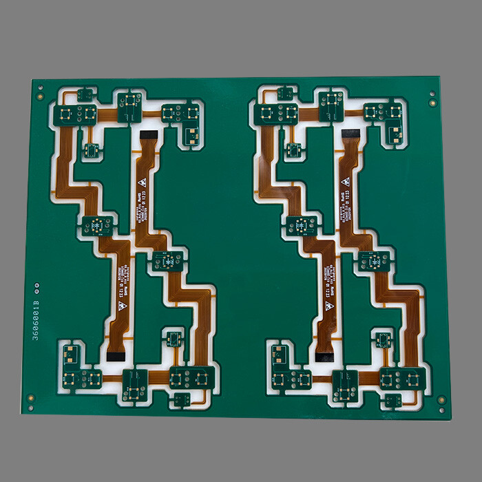


Commodity Name: Rigid-Flex Printed Circuit Board for Communication
Brand Name: HFast
Layers: 4L
Board Thickness: 0.10mm+1.00mm
Minimum Hole Size: 0.20mm
Minimum Line Width: 0.07mm
Minimum Line Spacing: 0.07mm
Surface Treatment: Gold Plating
Color: Yellow Rigid-Flex Film+Black Electromagnetic Film+ White Legend and Blue Rigid Board
Surface Treatment: Gold Plating
Advantages: 4layers soft hard bonding board, double-sided electromagnetic film shielding and 1 FR4 reinforcement.
Brief Introduction of Rigid-Flex PCB
Rigid Flex PCB is a hybrid structure circuit board that combines rigid PCB (such as FR4 material) and flexible PCB (such as polyimide PI substrate), and achieves three-dimensional interconnection through compression technology. It plays a key role in modern high-density electronic devices, especially suitable for scenarios that require a balance between mechanical strength and spatial adaptability.
The combination of soft and hard PCBs has become the core carrier for folding equipment, precision medical instruments, and intelligent vehicles due to its spatial reconstruction capability and dynamic reliability. Its design must strictly follow the wiring specifications for the rigid flexible transition zone (such as tear compensation, vertical bending direction), and balance material selection between cost and performance. In the future, with the popularization of ultra-thin adhesive free technology and innovation in hybrid materials, this technology will further evolve towards miniaturization (medical implant equipment), high-frequency (6G communication), and multifunctional integration (sensor+circuit integration), continuously promoting the revolution of electronic system form.
Characteristics of Rigid-Flex PCB
1. Combining rigidity and flexibility;
2. Ultra high space utilization rate;
3. Signal integrity optimization;
4. Strong resistance to environmental stress;
5. Lightweight and durable.
Deep analysis of structural design and manufacturing process of Rigid-Flex PCB
Typical stacked structure
|* * Level * *| * * Materials and Functions * * | * * Key Process Requirements * *|
|* * Rigid part * * | FR4 epoxy resin, providing mechanical support | Multi layer lamination, metalized via holes|
|* * Flexible part * * | PI substrate+rolled copper foil, achieving dynamic bending | Non adhesive substrate priority (low deformation coefficient)|
|* * Combining transition zone * * | Pre impregnated adhesive layer (such as acrylic adhesive) | Vertical bending direction of the wire to avoid right angle routing|
|* * Protective layer * * | Cover film (CVL) or photosensitive solder mask ink | Flexible area needs to be shielded from ink infiltration|
Manufacturing core difficulties and solutions of Rigid-Flex PCB
- Laminated deformation: The difference in thermal expansion coefficient between soft and hard materials leads to layer deviation - using non adhesive substrate, predicting shrinkage compensation design.
-Drilling pollution: Residual adhesive layer leads to failure of hole metallization
- plasma cleaning replaces chemical decontamination to ensure the cleanliness of the hole wall.
-Appearance machining burrs: The milling edge in the flexible area is prone to roughness - insert a rigid gasket for synchronous milling and control the tool speed.
-Ink leakage: Solder mask ink flows into the flexible area - the exposure film shields the flexible window, causing local solder mask.
Core Challenges and Future Trends of Rigid-Flex PCB
Current bottleneck
-Yield issue: The yield of multi-layer soft and hard boards is only 60-70% (traditional PCBs>95%);
-Design complexity: It is necessary to comply with both IPC-6013 (flexible board) and IPC-6012 (rigid board) standards simultaneously;
-Material limitations: The cost of PI substrate is 4 times that of FR4, and the price of rolled copper is 30% higher.
Technological Evolution Direction of Rigid-Flex PCB
1. Ultra thin adhesive free substrate: Laser direct forming (LDI) replaces the adhesive layer, with a thickness breakthrough of 0.05mm;
2. Mixed material system: PI/PET composite substrate balances cost and temperature resistance;
3. Integrated manufacturing: Embedded components (e-CAP), antenna integration (such as AiP design);
4. Green process: Lead free gold deposition and plasma etching replace chemical solutions.
Online Message
Application


CONTACT US
Please use the form below to get in touch.
If you need a reply we will get in touch as soon as possible.