
PRODUCT
PRODUCT
CONTACT US
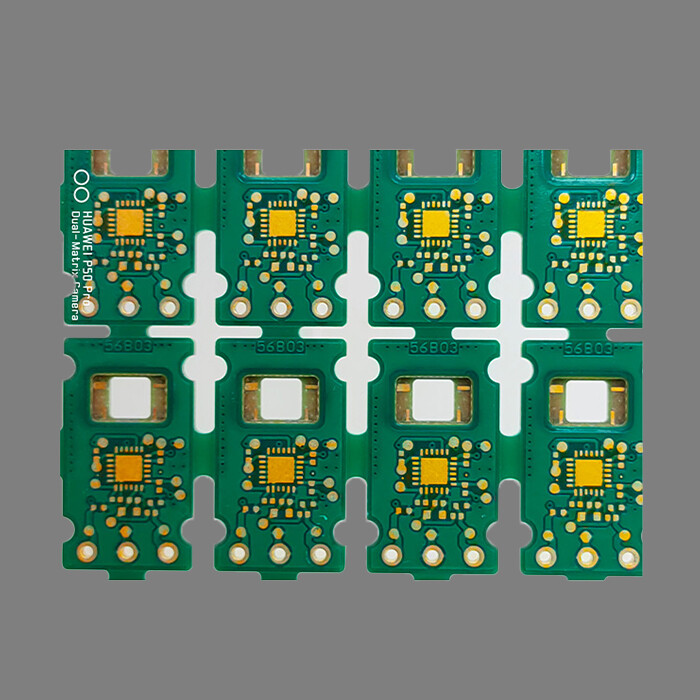


Commodity Name: Step ladder Circuit Board for Industrial Control
Brand Name: HFast
Base Material: Copper
Layers: 4L
Board Thickness: 1.60mm
Minimum Hole Size: 0.25mm
Minimum Line Width: 0.15mm
Minimum Line Spacing: 0.15mm
Surface Treatment: Immersion Gold
Color: Green Oil and White Legend
Advantages: The inner layer circuit PAD is gold-plated and made of PP hollow pressing without leaving glue. Component insertion soldering reduces the overall height of the PCBA and is protected by surrounding walls to avoid the risk of component impact
Brief Introduction of Step ladder PCB
Step PCB is a type of circuit board that achieves thickness differences in different areas through local milling or lamination control. It is designed specifically for three-dimensional space constraints, irregular assembly, or high-frequency impedance matching scenarios. Its core value lies in eliminating component height differences, optimizing structural space, and enhancing electromagnetic compatibility. It is widely used in precision equipment such as foldable screen smartphones, satellite payload modules, and medical endoscopes.
Core functions and advantages of Step PCB
|* * Application Requirements * * | * * Traditional PCB Pain Points * * | * * Step PCB Solution * * | * * Implementation Effect * *|
|* * Component height difference matching * * | Chip and connector height difference>2mm | Local milling thinning to component pad height | Whole machine thickness reduced by 30%|
|* * Alien space adaptation * * | Curved shell interferes with PCB edge | Step+side 45 ° chamfer embedded in cavity | Space utilization increased by 50%|
|Continuous high-frequency impedance | Sudden impedance change in connector area | Step controlled deep milling to dielectric layer to maintain impedance consistency | Signal reflection reduced by 80%|
|* * Optimization of heat dissipation channels * * | Gap between heat sink and chip | Step opening window+copper block flush chip | Thermal resistance reduced by 60%|
Irreplaceability:
>- Structural thinning limit: The thickness of the step area can be as low as 0.2mm (standard plate thickness 1.6mm);
>- Precision control: Step depth tolerance ± 0.05mm, angle tolerance ± 2 °;
>- Cost effectiveness Save 40% cost and reduce connector usage compared to stacked PCB solutions.
The three major structural types of Step PCB
1. Control deep milling step
|* * Parameters * * | * * Technical Points * * | * * Applicable Scenarios * *|
|* * Step depth * * | 0.1~1.0mm (accuracy ± 0.05mm) | Connector/chip height matching|
|* * Slope angle * * | 30 °~45 ° (laser cutting can reach 90 °) | Mobile phone camera module|
|* * Surface treatment * * | Selective gold/tin deposition in step area | Welding reliability|
2. Half cut step (V-Cut depth control)
-Process: Double sided V-cut (residual thickness 0.3mm) → Break after lamination
-Advantages: Achieving a vertical cross-section of 90 ° without burrs
-Limitations: Only applicable to board edge steps (such as folding screen hinge FPC exit)
3. Layered difference step
|* * Stacking scheme * * | * * Structure description * * | * * Performance characteristics * *|
|* * Asymmetric lamination * * | Region A: 6 layers → Region B: 4 layers (thickness difference of 0.8mm) | Accurate impedance control (± 5 Ω)|
|* * Mixed material embedding * * | Thin area: polyimide → Thick area: FR-4 | High frequency loss reduced by 50%|
Key Manufacturing Processes and Challenges of step PCB
1. Precision milling technology
|* * Difficulties * * | * * Traditional process defects * * | * * Innovative solutions * *|
|Copper foil tearing | Milling cutter pulling causes the edge of the step to curl | * * Laser ablation+chemical etching * * Combined process|
|Uneven depth * * | Milling depth fluctuation caused by board warping ± 0.1mm | Vacuum adsorption table+real-time thickness monitoring (accuracy ± 0.01mm)|
|* * Resin residue * * | Glass fiber burrs remaining on the bottom surface of the steps | Plasma etching (Ra<5 μ m)|
2. Laminated deformation control
-Material matching: CTE difference between thin and thick substrate<3ppm/℃ (e.g. IT-180A for thin area and FR-4 for thick area)
-Ladder style steel mold: Pre engraved step grooves on the compression mold, pressure balanced to 300psi
-Deformation compensation: Based on simulation pre scaling 0.05% graphics (such as Ansys Mechanical model)
3. Step area electroplating
|* * Process * * | * * Principle * * | * * Advantages * * | * * Limitations * *|
|Mask electroplating | Dry film covering non step areas | Thickness uniformity>90% | Easy to accumulate liquid at step corners|
|Pulse electroplating | Reverse current dissolution of protrusions | Surface flatness Ra<0.2 μ m | High equipment cost|
|Spray electroplating | Directional spraying of plating solution to step area | Excellent deep plating ability | Customized nozzle required|
The Golden Rule of Design of step PCB
1. Structural Design Specification
-Step depth: Maximum depth ≤ 70% of plate thickness (e.g. 1.6mm plate thickness step depth ≤ 1.12mm)
-Transition zone slope: Recommended for 40 °± 5 ° (laser cutting) or 30 °± 2 ° (mechanical milling)
-* * Safety distance * *: The distance between the edge of the step and the nearest wire is ≥ 0.3mm (tear resistant)
2. Key points of electrical design
-Impedance compensation: Step area line width adjustment formula:
$$W_{step} = W cdot sqrt{frac{H_{base}}{H_{step}}}$$
(W=original line width, H=dielectric thickness)
-* * Step crossing wiring * *: Right angle crossing is prohibited, and * * arc-shaped gradient wiring * * (curvature radius R ≥ 3W) is used
3. Hot Design Strategy
-Step heat dissipation window: Window opening in the step area corresponding to the high heating chip → copper block embedded (protruding height 0.1mm)
-* * Thermal conduction path * *: Fill the step area with thermal conductive silicone grease (thermal conductivity>5W/(m · K)) and directly connect it to the shell
Breakthrough direction of technique of step PCB
1. Laser composite processing
-UV laser+femtosecond laser combination: step depth control up to * * ± 0.01mm * *, slope angle adjustable from 10 ° to 90 °
2. Nano level interface bonding
-Step area magnetron sputtering titanium/copper transition layer → bonding force>1.5kN/m (anti delamination)
3. Additive Manufacturing Fusion
-Step surface inkjet printing of conductive silver paste → achieving * * direct connection of cross step components * * (resistance<5m Ω)
4. Intelligent compensation system
-Online 3D scanning+AI prediction of deformation → Real time adjustment of milling path (yield increased to 99%)
Online Message
Application


CONTACT US
Please use the form below to get in touch.
If you need a reply we will get in touch as soon as possible.