
PRODUCT
PRODUCT
CONTACT US
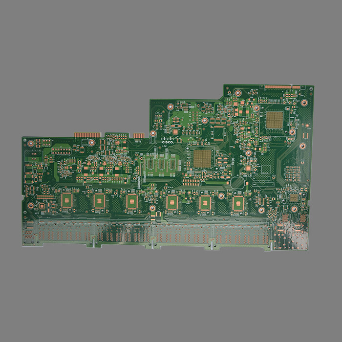
Commodity Name: Communication Server Printed Circuit Board
Brand Name: HFast
Layers: 8L
Board Thickness: 1.60mm
Minimum Hole Size: 0.20mm
Minimum Line Width: 0.076mm
Minimum Line Spacing: 0.076mm
Color: Green Oil and White Legend
Surface Treatment: Gold Plating
Remark: OEM for Cisco Server
Key Characteristics of Communication PCB
1. Core: Selection of Special Materials
*High frequency/high-speed substrate (crucial!):
*Rogers Series: Industry benchmarks (such as RO3000, RO4000, RT/duroid). Ceramic filled PTFE substrate with extremely low loss, stable dielectric constant, and low moisture absorption. High cost, used for critical RF links and high-speed digital channels.
*Taconic series: Similar to Rogers, it offers a variety of high-performance materials (such as TLY, RF-35), which may have slightly better cost-effectiveness.
*Isola, Panasonic, Nelco, etc. provide mid to high end high-speed materials such as ISOLA I-Speed and FR408HR; Panasonic Megtron 6/7/8; Nelco N4000-13/29)。 Excellent performance, lower loss than standard FR-4, and lower cost than pure PTFE material, widely used in high-speed backboards, server motherboards, and network equipment core boards.
Modified epoxy resin/special filler FR-4: In areas with less extreme or cost sensitive requirements, use medium loss materials (better than standard FR-4).
*Ceramic substrate: Used for extremely high power or high-frequency millimeter wave applications (such as GaN amplifiers).
*Copper foil:
*Low roughness copper foil: At high frequencies, the surface roughness of copper foil significantly increases conductor loss. HVLP (Ultra Low Profile), RTF (Reverse Processing) or more advanced copper foils are necessary.
*Solder mask: Low loss, low dielectric constant, high heat resistance, and good adhesion are required. Significant impact on high-frequency regions.
*Surface treatment:
*Nickel immersion gold: The mainstream choice. Good flatness, suitable for fine pitch BGA soldering, stable contact resistance, and oxidation resistance.
Sinking Silver:The signal loss is slightly lower than ENIG (with one less layer of nickel), and the high-frequency performance may be slightly better, but it is prone to oxidation and vulcanization, and long-term reliability needs to be paid attention to. The weldability is slightly worse than ENIG.
*OSP: The lowest cost, good signal integrity (pure copper surface), but poor protection, short solderability retention period, only used for non critical, easy to weld, and short production cycle boards.
*Electroplated hard gold: Used for gold fingers with high wear resistance requirements (such as backplane connectors).
2. Design: Precise Layout and Wiring
Strict partitioning: * * Clear division of digital, analog RF、 High speed and power supply area.
*Stacking design: Carefully plan the stacking structure to ensure the continuity of the signal reference plane (ground or power), control impedance, and provide a low impedance return path.
*Differential pair wiring:
*Strictly equal length, equidistant, and symmetrical routing.
*Avoid unnecessary vias (increasing impedance discontinuity and losses).
*Maintain sufficient spacing from other wiring/structures to reduce crosstalk.
*Optimization of via design:
*Try to minimize the number of through holes, especially on critical high-speed paths.
*Use a back drill to remove excess copper posts (Stubs) and reduce signal reflection and loss.
*Optimize the via structure (size, solder pads, anti solder pads) to reduce impedance discontinuity and parasitic effects.
*Power integrity design:
*Use multi-layer boards to provide a complete power/ground plane.
*Carefully design decoupling capacitor networks (with different capacitance values and positions).
*Power layer segmentation may be used, but attention should be paid to cross segmentation issues.
*EMC design:
*Add shielding covers to critical areas.
*Sensitive signal line grounding treatment.
*Use a grounding via array (Via Fence) at the edge to suppress edge radiation.
*Filter circuit design (at power inlet and interface).
3. Manufacturing: High precision and strict control process
*HDI process: laser drilling (micro hole), sequential lamination, fine line etching (≤ 4mil line width/line spacing), hole filling electroplating (VIPPO).
*High precision alignment: The interlayer alignment accuracy requires extremely high precision (especially for HDI boards).
*Impedance control: achieved through strict control of dielectric thickness, copper thickness, line width and spacing.
*Backdrill: Remove the unused copper pillar portion (Stub) on the high-speed signal via.
*Advanced surface treatment: Ensure uniformity and thickness control.
Strict testing:
*AOI: Automatic optical inspection for circuit defects.
*Impedance testing: Sampling or flying pin testing of key line impedance.
TDR testing: Time domain reflectometer tests signal integrity.
X-Ray: Check BGA soldering, buried holes, etc.
*Slicing analysis: Check the quality of copper holes and the microstructure of laminated bonding.
Online Message
Application


CONTACT US
Please use the form below to get in touch.
If you need a reply we will get in touch as soon as possible.