
PRODUCT
PRODUCT
CONTACT US
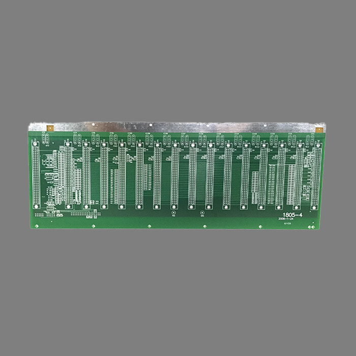
Commodity Name: UPS Power Bank Printed Circuit Board
Brand Name: HFast
Layers: 4L
Board Thickness: 1.60mm
Minimum Hole Size: 0.30mm
Minimum Line Width: 0.30mm
Minimum Line Spacing: 0.30mm
Color: Green Oil and No Legend
Surface Treatment: Lead Free HASL
Brief Introduction of UPS Power Bank PCB
The power bank PCB also called the energy storage system PCB is the core hardware platform that supports the safe, efficient, and intelligent operation of battery energy storage systems. They carry key functions such as battery management, energy conversion, system monitoring, safety protection, and communication, and are indispensable "brains" and "neural networks" for modern energy storage power plants (large power plants, industrial and commercial energy storage, household energy storage) and portable energy storage devices.
Characteristics of Energy PCB
1. High power carrying capacity;
2. High voltage isolation and safety design;
3. Strong thermal management capabilities;
4. High reliability and long lifespan;
5. Complex signal integrity and anti-interference design;
6. Multi layer design;
7. Large size and special structure;
8. High density connectors;
9. Test points and maintainability.
Key components and technical characteristics of energy storage PCB
1. Core PCB type:
BMS main control board: the system's "brain", including the main control MCU/MPU, communication interface, storage, clock, etc. Responsible for data processing, strategy execution, system monitoring, and external communication. The number of layers is usually 4-8.
BMS control board: installed on battery modules or clusters, responsible for collecting individual battery voltage/temperature and performing passive balancing. The number of layers is usually 2-6. Require high-precision analog circuit design.
The high-voltage sampling and isolation interface board is specifically responsible for high-precision sampling of total voltage and total current, and provides isolation communication channels between the high-voltage and low-voltage sides. The requirements for isolation withstand voltage and sampling accuracy are extremely high.
Relay drive and status monitoring board: Drive high-voltage relays/contactors and monitor their status (adhesion, contact status).
Auxiliary power board: provides isolated and stable low-voltage power supply (such as 24V, 12V, 5V, 3.3V) for the entire BMS system.
Display/human-computer interaction board: used to display system status and set parameters (commonly seen in household energy storage).
2. Selection of key materials
Substrate:
High reliability FR-4: mainstream choice, using high Tg (≥ 150C, preferably 170 C), low CTE high CAF resistance halogen-free materials (such as Isola FR408HR, Panasonic Megtron 4/6, Shengyi S1000-2M, ITEQ IT-180A)。 Meet long-term reliability and safety requirements.
Ceramic substrate/metal substrate: used for power devices that require extremely high heat dissipation or high insulation locally (such as high current balanced MOSFETs).
Copper foil
Signal layer: standard 1oz copper.
Power supply/power layer: Thick copper foil (2oz, 3oz) is necessary for carrying high current paths (main circuit sampling resistors, relay connections, balancing circuits).
Solder mask: requires high heat resistance, high adhesion, excellent chemical resistance (corrosion resistance), and high insulation strength. The colors are mostly green or black.
Surface treatment:
Nickel immersion gold: preferred. Provide excellent solderability, flatness (suitable for precision ICs), oxidation resistance, and long-term reliability. The gold layer performs well at weak signal contact points.
Tin deposition: Low cost and good solderability. Assess the risk of tin whiskers and their long-term reliability in high temperature and high humidity environments.
OSP: The lowest cost, but it is less commonly used in energy storage PCBs that require high reliability and may require multiple soldering.
Silver deposition: Good signal performance, but prone to sulfurization and blackening. It should be used with caution or protected with a coating in sulfur-containing environments (some industrial scenarios).
Localized gold plating: used for critical testing points or connector contacts.
3. Design points:
Layout partition: Strict physical isolation!
*High voltage power zone: Main circuit sampling resistor, relay contact, fuse, high voltage connector. **Maintain sufficient spacing! Slotting increases creepage distance!
*Low voltage simulation area: Battery cell voltage sampling, temperature sampling (NTC), reference voltage source, precision operational amplifier/ADC. Stay away from noise sources and prioritize protection! Use a shielding cover or wrap around the ground.
*Digital control area: MCU, communication interface, logic circuit.
Power area: Switching power module LDO、 Filter capacitor.
*Sampling circuit design:
*Kelvin connection: Kelvin connection (four wire system) must be used for sampling resistors (especially current sampling resistors) to eliminate the influence of wiring resistance.
*Short and thick sampling line: The voltage sampling point should be as close as possible to the battery pole, and the wiring should be short and thick. Differential wiring should be used to reduce common mode interference.
Filtering and Protection:RC filtering and TVS/ESD protection devices are added to the sampling input.
Thermal management:
Balanced resistor heat dissipation: Passive balanced resistors are large heat sources that require large-area copper skin heat dissipation and heat dissipation holes, and heat dissipation fins may be added if necessary.
*Power device heat dissipation: Relay driven MOSFETs and DC/DC power devices require good heat dissipation design (heat dissipation pads, thermal conductive holes, heat sinks).
*Layout: Avoid concentrating heat sources.
*Grounding design:
*Star grounding or mixed grounding: Analog ground, digital ground, power ground, and enclosure ground are connected at a single point to avoid introducing noise into the ground loop.
*Complete grounding plane: The multi-layer board provides a low impedance grounding plane.
*EMC design:
Filtering is everywhere: * * Add filtering (common mode inductance, magnetic beads, capacitors) to the power inlet, communication interface, and signal line inlet.
Shielding:Use shielding covers for critical analog circuits and high-speed digital circuits.
Via array:Grounding via array is arranged around the board edge and sensitive signals to form an electromagnetic shielding wall.
Optimize switch circuit: Minimize the area of power circuit (especially high-frequency switch circuit).
Online Message
Application


CONTACT US
Please use the form below to get in touch.
If you need a reply we will get in touch as soon as possible.