
PRODUCT
PRODUCT
CONTACT US
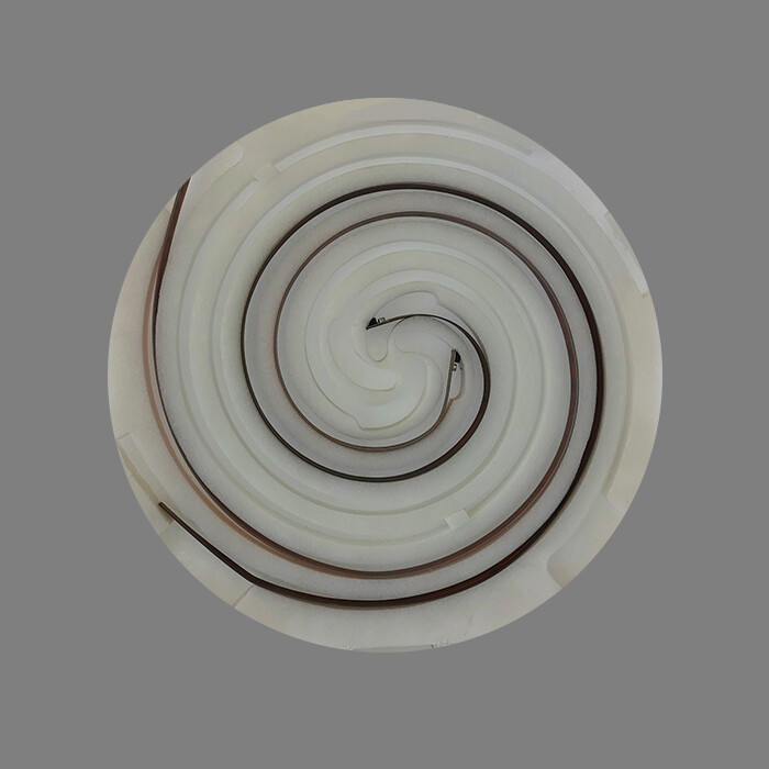
Commodity Name: MRI(Magnetic Resonance Imaging) Printed Circuit Board
Brand Name: HFast
Layers: 2L
Base Material: Teflon PTFE
Board Thickness: 1.60mm
Minimum Hole Size: 0.50mm
Minimum Line Width: 0.50mm
Minimum Line Spacing: 0.50mm
Surface Treatment: Gold Plating
Challenges and Development Trends Faced by Medical Electronic PCB
1. Challenge:
*Balancing cost and ultimate requirements: Meeting ultra-high reliability and regulatory requirements results in significantly higher costs than ordinary PCBs.
Increased technical complexity: Equipment miniaturization, intelligence, and multifunctionality pose higher requirements for PCB design (HDI, rigid flexible combination, embedded components) and manufacturing processes.
*Regulatory updates and compliance pressures: Global medical device regulations (such as EU MDR/IVDR) are constantly being updated and tightened, resulting in high compliance costs.
*Supply chain security and stability: The supply chain of critical materials and components (especially those that meet medical grade standards) needs to be highly reliable.
*Long term support: Medical equipment has a long lifecycle, and it is necessary to ensure the long-term supply and substitutability of components and PCBs.
2. Development Trends:
Higher density interconnection:Widely using * * HDI technology * * (micro holes, blind buried holes), * * rigid flexible combination board * *, to achieve device miniaturization and portability (such as wearable devices, endoscope probes).
*Integration and modularization: Integrate more functions onto smaller PCBs or adopt modular design for easy upgrading and maintenance.
*Wireless connectivity and IoT: Wearable devices and remote monitoring devices drive the integration of low-power Bluetooth, Wi Fi, NB IoT, and other wireless communication modules on PCBs.
*Advanced sensing technology integration: Integrating biosensors more tightly onto PCBs (such as the prototype of Lab-on-a-PCB).
*The application of artificial intelligence at the edge: Integrating AI acceleration chips on PCBs to achieve localized real-time data processing and diagnosis.
*New Material Applications: Explore substrates, coatings, and interconnect materials that are more high-performance, environmentally friendly, and biocompatible.
*Exploration of additive manufacturing: The potential application of 3D printed electronics in customized, rapid prototyping, and small batch special medical equipment PCBs.
*Predictive maintenance and status monitoring: Integrate sensors on the PCB to monitor its own health status.
Online Message
Application


CONTACT US
Please use the form below to get in touch.
If you need a reply we will get in touch as soon as possible.